Oxford, UK and Tokyo, Japan, November 18, 2026
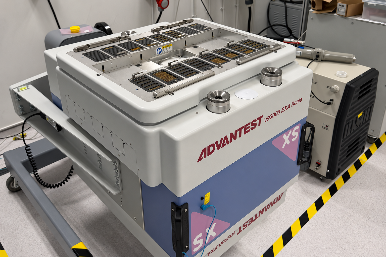
EnSilica, a leading maker of mixed-signal application-specific integrated circuits (ASICs), has taken delivery of Advantest’s V93000 EXA Scale SoC Test System to be used for the testing of high-performance mixed-signal and RF devices. The latest-generation EXA Scale from the leading supplier of semiconductor test equipment has been installed at EnSilica’s site in Oxford, UK.
The on-site tester system strengthens EnSilica’s ability to support its growing pipeline of ASIC and ASSP products as they progress from development into volume production. It provides advanced test capability across high-speed digital, RF, analogue and mixed-signal devices and will be used for test development, silicon validation and product qualification.
Investing in the EXA Scale helps to enable EnSilica’s continued expansion of its end-to-end ASIC design and supply capabilities. In addition to semiconductor design and development, EnSilica manages the complete supply chain for customers, including wafer manufacture, packaging, production test and delivery of finished semiconductor devices.
The V93000 EXA Scale platform provides superior throughput and scalability, together with advanced RF performance and wider frequency coverage. Its flexible architecture enables EnSilica to develop test solutions for increasingly complex and highly integrated devices combining digital, analogue, RF and mixed-signal functionality.
Direct access to the latest-generation test platform will allow EnSilica’s engineering and operations teams to develop, debug and optimise production test programmes more quickly. This will help accelerate the industrialisation of new products and increase EnSilica’s capacity to support the growing number of ASIC programmes expected to transition into production over the coming years.
The platform will also enable test programmes to be continually optimised as products mature and production volumes increase. Reducing test time and improving test efficiency can make an important contribution to lowering unit manufacturing costs, allowing EnSilica to manage the cost of test throughout the lifetime of each product.
The additional capability will support EnSilica’s growing portfolio of customer-funded ASIC programmes and its own ASSP products across the space and adjacent markets. It further strengthens the Company’s ability to support customers throughout the complete semiconductor lifecycle, from architecture and ASIC design through test development and qualification to long-term volume supply.
Olivia Slater, VP of Operations & Quality at EnSilica, commented:
“We have a growing pipeline of ASIC and ASSP products progressing towards production, and expanding our test development capability is an important part of supporting that growth. Our work with Advantest gives us direct access to the latest-generation V93000 EXA Scale platform here in Oxford, which will allow our teams to develop and debug production test solutions faster and more efficiently, helping us accelerate new products from first silicon into volume production.
As those products move into higher volumes, we can continue to optimise their test programmes to reduce test time and improve manufacturing efficiency. This allows us to control test costs throughout the lifetime of a product and strengthens our ability to provide customers with a complete semiconductor solution from initial development through to long-term volume supply.”
“Advantest is pleased to expand its long-standing relationship with EnSilica, supporting innovative ASIC development through the next-generation capabilities of the V93000 EXA Scale platform,”
Said Stefano Ermolli, VP of Customer Relations, Advantest Europe. He added:
“Combining best-in-class throughput with advanced digital, mixed-signal and RF performance, the EXA Scale is designed to meet the demands of increasingly complex semiconductor devices. Its scalable architecture provides the flexibility to evolve alongside EnSilica’s growing ASIC portfolio, while the platform’s broad adoption across leading OSATs worldwide enables a seamless path from development and qualification to high-volume manufacturing. Together, these capabilities create a strong foundation for continued collaboration and help bring advanced semiconductor solutions to market more efficiently.”