Design Services

Our Offer
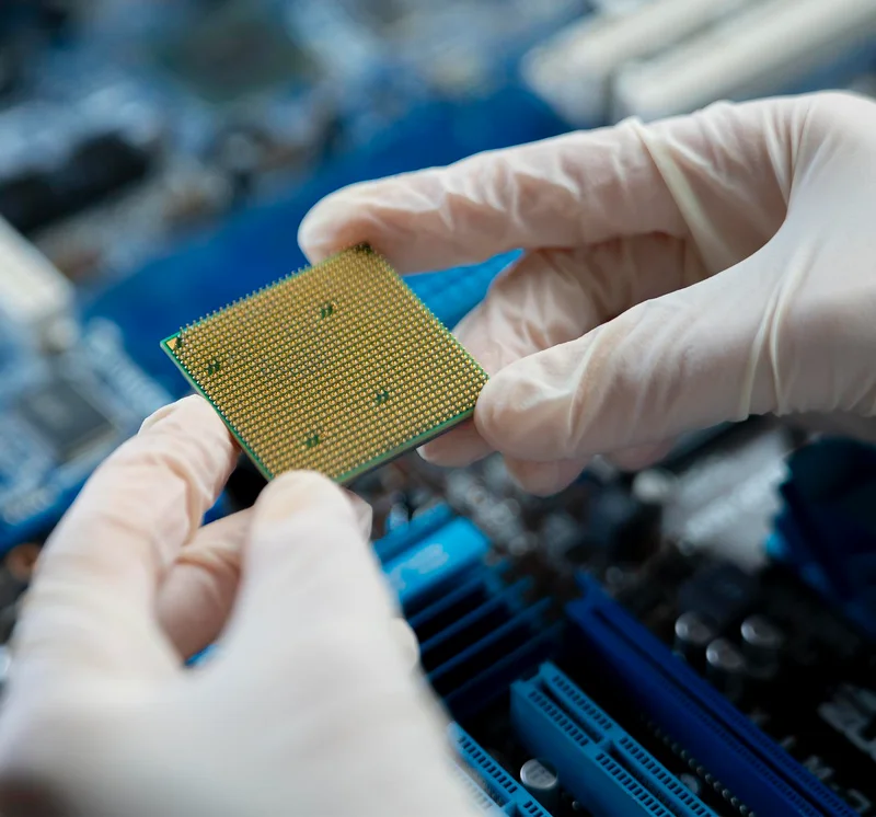
EnSilica offers advanced semiconductor design services for ASIC, SoC, and FPGA developments across a range of demanding applications.
Our expertise covers full turnkey development, specific IP or sub-system design, and seamless team augmentation for semiconductor and electronics companies.
Benefits
Why EnSilica for your design services needs
Flexible engagement: full turnkey or customer team augmentation options
European and offshore design centers for efficient project delivery and cost-effectiveness
Deep expertise with industry-leading EDA tools, IP, and foundries worldwide
Proven success across digital, analog, RF, and mixed-signal designs for global clients
We always put customer's demands first and care about the customer's final product
We can work with you on ‘how’ to develop your solution, but also will use our expertise to help you in shaping the "what"
Vast amount of experience accumulated by the team, whose turnover is one of the lowest in the industry
End to End Capabilities

Get in touch with our Design Services experts
Our Design Services methodology
End to end services tailored to your needs
System-Level Design
- Development of system architectures from initial marketing requirements through to detailed technical specifications
- Specialist expertise in RF and control systems modeling
- Creation of executable models to validate architectures prior to hardware implementation
Design & Verification
- RTL design for networking, wireless, and radar applications
- Conversion of MATLAB/SystemC models into hardware implementations
- Comprehensive verification using UVM with SystemVerilog, coverage-driven methodologies, and industry-standard verification IPs
Physical Implementation & DFT
- Full RTL-to-GDSII flow, supporting mixed-signal and hierarchical ASICs from block to full-chip
- Extensive experience using premier EDA tools: Synopsys IC Compiler II, Cadence Innovus, Siemens Tessent Suite, and Siemens Calibre
- Proven execution across advanced nodes (350nm down to 12nm FinFET, FD-SOI)
- Partnerships and design tape-outs at leading foundries, including TSMC, GlobalFoundries, UMC, SMIC, and Key Foundry
- Specialized in low-power design (UPF), RF IP (Wi-Fi, BLE), high-speed SerDes, and precision data converters
Analog Design & Layout
- Ultra-low-power SoC and IP design for advanced radios and power management—processes down to 7nm
- IP library: sensor interfaces, ADCs/DACs, voltage regulators, clocking solutions, BLE radios, NFC analog front ends
- Notable projects: Ka-band mmWave RF ASIC (40nm), industrial radio ICs (350nm SiGe), automotive H-Bridge controllers (180nm BCD)
Embedded Software
- Firmware and driver development for pre-silicon verification and post-silicon validation
- Production software for Arm Cortex, Tensilica ConnX, NVIDIA GPUs
- Support for Embedded Linux, Arm Mbed, Micrium uC/OS-III, FreeRTOS, and bare-metal systems
- Delivered solutions for automotive radar, LoRaWAN IoT modules, functional safety controllers, and mobile connectivity products
- V-model design and testing for safety-critical applications
Silicon Validation
- In-depth validation of ASICs across corners (process, voltage, temperature)
- Automated test systems using LabVIEW, LabWindows, and Python frameworks
- In-house FPGA platform for advanced Scan/MBIST validation pre-production
- Comprehensive lab capabilities: oscilloscopes, spectrum/signal/logic analyzers, environmental testing chambers
Discover more
See examples of our successful projects
Our offer
Check what else we can do for you
Turnkey ASIC

Manufacturing Services

Products (ASSP)