Manufacturing Services

Why Manufacturing Services with EnSilica
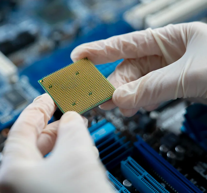
EnSilica is a trusted partner for semiconductor manufacturing, offering flexible delivery models and deep experience across the full production flow, from tape-out to tested, qualified packaged parts or just wafer supply.
Direct partnership with the leading foundries
Direct access to all the leading fabs including TSMC, GlobalFoundries, ST Microelectronics.
Turnkey ASIC Manufacturing
One partner for specification, design, verification, manufacturing, packaging and testing.
Advanced Node Expertise
Proven success with a range of technologies including FinFET down to 6nm with 4nm currently in design.
Global Engineering Support
Teams across the UK, EU, US and Asia.
Dedicated Project Management
One point of contact from start to volume ramp
Flexible Engagement Models
One point of contact from start to volume ramp
Process steps
Manufacturing Services at EnSilica

Design
- IP Access
- Full Design from Customer Spec
- Customer RTL Design Integration
- DFT, Physical implementation
Test
- Test Strategy including Tester Selection, multi-site, ATE & Probe
- Test Solution Development, Hardware & Software
- Test Plan, Debug & Characterization
- Yield Optimization
Fab
- Multi Project Wafer Tapeout
- Production Mask Tapeout
- Tapeout Support Including DRC, Mock Tapeout, Foundry Support
- WAT Data
Qualification
- Including Automotive, Customer, Industrial Standards (AEC-Q100, JEDEC)
- Qualification Strategy, Reliability Plan & Report
- Management of Manufacturing & ATE Test Readpoints
- Failure Analysis
Assembly
- Package Selection Support
- Package Feasibility & Design for Manufacturing
- Prototype
- Mass Production
Production
- New Production Introduction
- Logistics
- Order Entry
- Supply Chain Management, WIP
Reports
Get in touch with our Manufacturing Services experts
Our offer in detail
What do we do
We offer a cohesive suite of manufacturing services that ensures a seamless transition from design to high-volume, reliable semiconductor production.
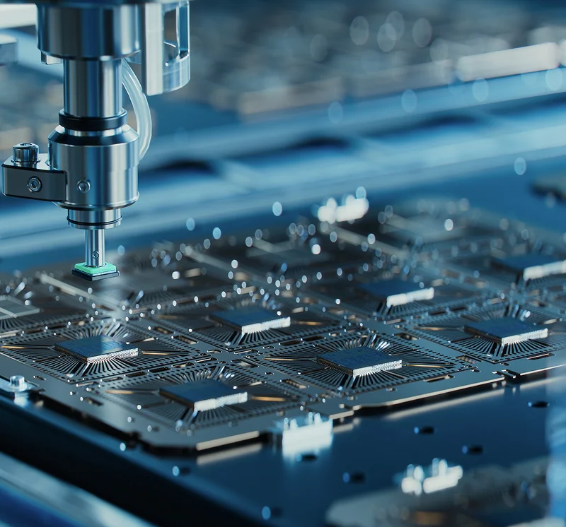
Foundry Tape-out Services
EnSilica provides full support for ASIC tape-out and access to a broad range of foundries and process technologies.
- Foundry Access – We support tape-outs at TSMC, GlobalFoundries, X-Fab, SK keyfoundry and STMicroelectronics. Our flows can be adapted to other foundries as needed
- Process Coverage – Support for nodes from 600nm to 6nm FinFET, across standard CMOS and advanced technologies
- Tape-Out Process – We manage PDK setup, design rule checks, sign-off, and mask ordering using standard EDA tools, aligned to each foundry’s requirements
- Experienced Team – Our engineers have delivered recent tape-outs across multiple foundries, using established processes that can scale across technologies
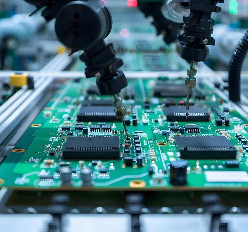
Packaging Design and Assembly Services
EnSilica manages the full ASIC packaging design process, from customer requirements definition to assembly partner selection and production
- Requirements Analysis – We begin with a detailed assessment of application needs, including size, thermal limits, lead pitch, performance targets, cost, and industry standards.
- Package Type Selection – Package choice is driven by technical constraints and use case. Options include leaded, leadless, flip-chip, wirebond, WLCSP, and substrate-based packages
- Design Specification and Supplier Feasibility – A complete package specification is created, followed by supplier selection. We perform feasibility checks and review all design parameters against manufacturing constraints.
- Assembly Partner Engagement – We work with trusted OSATs, including ASE and Unisem, to implement the selected package design and support volume production
Production Test Development
Test development is built into our manufacturing process to support consistent, production-ready ASICS
- Qualification Support – We support customer-specific qualification requirements, including AEC-Q100 for automotive-grade products.
- Custom ATE Development – Our engineers develop custom ATE software to maximise test efficiency and coverage at both wafer and package level, across the full operating temperature range.
- Final Test and Packaging – We provide visual inspection, tape-and-reel, and dry-pack (moisture barrier bag) services to ensure products are ready for shipment.
Quality and Reliability
At EnSilica, our commitment to quality is central to everything we do.
- In the semiconductor industry, precision and reliability are essential, which is why our manufacturing services are built around robust quality processes at every stage.
- From product qualification and environmental testing to final production, we ensure every ASIC meets industry standards and consistently delivers on customer expectations
Test Platforms
EnSilica supports production test across a range of ATE platforms, selected based on device type, performance and cost targets
Our Offering
Check what else we can do for you
Turnkey ASIC
Design Services
Products (ASSP)