Advanced ASIC Verification

EnSilica provide a comprehensive range of ASIC verification services to help our customers achieve working silicon first time around.

Verification represents one of the biggest challenges facing IC developers getting their design into the market within acceptable timescales.

Silicon technology continues to advance – providing increasing scope to integrate a wide range of IP including digital / analog cells, embedded processors, memories, high speed IO, in-house / 3rd-party IP etc onto a single device.   Traditional verification techniques (e.g. directed testing) simply cannot cope with this complexity.

This is where EnSilica verification consultants can help. We understand the challenges presented by these designs and work with our customers to provide everything from in-depth knowledge to solve a specific verification problem, to delivering a comprehensive verification solution for a complete chip.
Some of the methodologies and techniques we employ are given below, or just contact us to discuss your specific design requirements.

UVM logo
system verilog logo

ASIC Verification Services

  • Verification Capabilities

    Just some of the areas where EnSilica have expertise that could be applied to your project:

    • Verification planning, feature extraction, capturing functional coverage and check points
    • Architecture support of UVM
    • Assertion-based verification using SVA
    • Metric driven verification techniques using advanced tools to increase the verification confidence
    • Formal verification techniques
    • Verification IP (VIP) developments
    • Integration of third party IP
    • Creation of wrappers and multi-language interface sockets
    • Creation of reference models using traditional HDL languages and advanced HVL languages like System Verilog, C, C++ and System C
    • Regression management
    • FPGA prototyping, emulation platforms and system demonstrators
    • Low-power verification techniques – power estimation, CPF/UPF
    • Gate level simulation
    • Register abstraction based flow enabling design and verification reuse
    • Design of always-on agents and protocol checkers
    • Cycle accurate C modelling of module and complete systems
    • Use of PLI for co-simulation of embedded processors
    • End-to-end verification closure from specification to RTL signoff
  • Verification Planning and Strategy

    The key to a successful verification project is in the planning …  ‘failing to plan is planning to fail’.  However, for many customers the complexity of the verification challenge can be daunting – particularly if it has been some time since the last tape-out and EDA tools and methodologies have moved on.

    This is where EnSilica can help.

    EnSilica employ a structured verification flow (see section below),  where the first step is a comprehensive planning phase. Based on the experience gained across multiple projects and many different application areas, we can define a comprehensive verification strategy utilising the best design practises within the industry and the latest design methodologies, whilst leveraging any knowledge or existing verification techniques available within your company.

    Some of the considerations taken into account include:

    • Specification review – identifying the key features/modules to be verified and the most appropriate approach for each one
    • HW / SW co-verification techniques
    • Availability of in-house ‘legacy’ verification techniques/knowledge
    • Possible use of in-house or 3rd-party Verification IP  (VIP)
    • Consideration of UVM
    • Recommendations on choice of EDA tools and flows
    • Consideration for module, sub-system and chip-level verification
    • Special requirements e.g. mixed-signal design, low power (upf, cpf), safety critical (e.g. ISO26262) etc
    • Resources, schedule , costs to implement the verification strategy

    The clarity afforded by this approach ensures that before the project even kicks-off, the scope of the verification challenge is understood and there are solutions identified. This delivers the most efficient implementation and increases confidence in both the quality and predictability of the schedule.

  • EnSilica Verification Flow

    EnSilica adopt a structured approach to the planning and execution of verification on a module or complete design

    • Planning Phase:
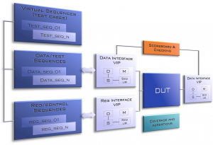
      The specification is reviewed and a verification plan document generated. The verification plan captures the required features that must be checked by the verification activities (RTL functional verification, FPGA prototyping, emulation, formal techniques etc).  In addition, it includes details of the test environment (e.g. UVM) showing how it is architected and demonstrating that it provides the mechanisms necessary to exercise the DUT in all its modes and corner cases, along with details of the testcases etc.
    • Phase 1:
      The focus here is on the creation of a working test environment. A basic (sanity) test passes and it can be shown that the test environment architecture meets all the requirements of a scalable, modular test environment which can then be extended to drive up the coverage with both scoreboard and assertion based checking. The verification plan is enhanced and becomes the record against which the completeness of the verification is reported.
    • Phase 2:
      In this phase the test environment is completely coded including cover points, checkers and assertions. This is the main phase for the creation of test cases, bug identification and fixing. Regular regressions will be run and the code and functional coverage pushed up to ~95% giving high confidence that the design is robust and that the test environment can fully exercise the module.
    • Phase 3:
      During this phase the remaining coverage holes are tackled and bug fixes implemented. When all testcases pass, functional and code coverage goals are achieved (100%), bug rate discovery is zero (and has been for at least a complete cycle of all the testcases) and there are no outstanding bugs to fix.  The verification can be considered complete.

“EnSilica have applied  a range of advanced techniques to address the verification challenges of these devices and ensure the successful delivery of  high quality silicon. Throughout the projects, EnSilica have demonstrated flexibility and commitment to the projects providing a mix of on-site / off-site support and the ability to adjust the size of the team based upon the demands of the projects – to allow projects to continue in parallel or provide  additional resource at key phases of the projects to ensure that tapeout dates are achieved.”

Stuart Levine Director of Engineering, Dialog Semiconductor
verification flowchart
© Copyright - EnSilica | Privacy Notice | Call Us - UK General : +44 118 321 7310 - UK Sales : +44 118 380 5757 - USA : +1 855 642 1070 - India : +91 80 2258 4450