IoT and Consumer : ASIC Design and Supply

The IoT and consumer markets are well serviced by standard electronic parts but when you need to differentiate your product due to the need for enhanced or novel functionality, a smaller form factor, increased security or a longer battery life, then a custom ASIC can offer a cost-effective solution to meeting these requirements.

EnSilica have the expertise in wireless, low-power, security and embedded processor integration to be the ideal partner to work with you to develop a custom ASIC solution that meets your requirements, and we can also manage the supply chain, from first silicon to volume production.

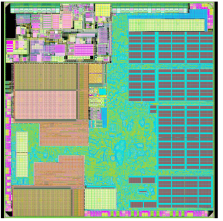
edge processor plot

Sensor interface edge processor
in 55nm eFlash

ensilica custom asic chip

Advances in ASIC Technologies

Recent advances in ASIC technologies make it possible to integrate all the functionality required to bring next-generation IoT and Consumer designs to market, including; low-power design, custom sensor and control interfaces, wireless/wired connectivity, embedded security and ai and machine-learning.

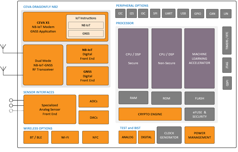
eSi-NB-IOT: Smart Sensor ASIC Platform

Highly integrated, specialised sensors with a low power NB-IoT modem for remote monitoring and control

The eSi-NB-IOT-Sensor is a customisable SoC platform delivering a fully integrated NarrowBand-Internet of Things solution that is compliant with the 3GPP Release 14/15 Cat NB2 standard. The modem is based on the market leading CEVA Dragonfly NB2 solution with an optionally integrated GNSS capability.

Connectivity – RF and Wireless

Our skilled RF and digital silicon engineers can integrate a wide range of wireless connectivity solutions into an ASIC design, using both in-house connectivity IP and solutions from our partners and suppliers. Our design teams have in-depth experience designing or integrating; Bluetooth Classic, BLE, NFC/RFID, WiFi (802.11), LoRa and NB-IoT.

Low-Power

EnSilica has extensive expertise in the design of low Power ASICs and SoCs, including for wireless connectivity and global positioning systems (GNSS). We are experienced in the use of multiple mode operations using power gating, voltage and frequency scaling, and low duty cycle operation modes as well as designing for near threshold voltage operation using DC-DC converters in order to maximize power efficiency when running from a battery.

Embedded Security

With the ever-increasing threat of cyber-attacks comes the need to ensure any connected device is sufficiently protected so that its operation is not disrupted, and the attack does not compromise safety, data security or profitability.  EnSilica has access to a broad library of internal hardware cryptographic accelerator IP, as well as from 3rd party IP suppliers, and will can also integrate security solutions from our partners such as Rambus and Arm to ensure we deliver the highest level of security, including:

  • Firmware integrity and secure boot
  • Secure, mutual authentication for device identification
  • Secure Communication with end-to-end encryption
  • Security life-cycle management
  • Tamper and side-channel attack protection

Edge Processing and AI

The trend is for the “thing” in the Internet of Things to get smarter and we work with a range of processor and IP partners to ensure we select and deliver the most appropriate smart processor core or DSP to meet each device’s specific requirements. There is also an increasing trend for adding artificial intelligence (AI) or machine learning (ML) to devices. The majority of arithmetic operations needed for neural network inference are matrix-vector multiplies which can be implemented in processors with SIMD extensions and DSP cores from the likes of CEVA and Tensilica. Recent advances in AI/ML have led to a range of NNAs being developed by our IP partners which can be integrated into edge devices for smart processing of data from audio, video, Radar, vibration or motion sensors.  IP suppliers for NNA include Arm, Imagination Technologies, CEVA and Tensilica, our engineers have the skills and experience necessary to integrate these IPs into a SoC design alongside a conventional processor, DSP and/or GPU core.

EnSilica – Simplifying Your Path to ASIC Deployment

EnSilica’s engineers live and breathe ASIC development every day and apply their in-depth knowledge to ensure that every project meets its requirements and is delivered on-time, on budget and right first-time.  Our wealth of experience combined with our Custom ASIC and full-flow ASIC Design Services enable OEMs and IC design teams to overcome the challenges in complex ASIC design, including:

  • Increasing design complexity and timescale pressure
  • Advances in silicon process capability
  • Performance, cost, and power optimisation
  • Verification complexity and coverage
  • IP selection and integration
  • New EDA tools and methodologies

Article: The Economics of ASICs: At What Point Does a Custom SoC Become Viable?
Article: ASICs for implementing functional safety in battery-powered home appliances

ASIC Benefits

  • Reduced BOM
  • Increased performance
  • Lower power consumption
  • Added functionality
  • Enhanced security
  • Smaller size and weight
  • Improved IP protection
  • Improved yields
  • Reduced test and assembly costs
  • Improved Reliability

Find out more

If you are looking for an IoT or Consumer ASIC development and supply partner with the right expertise and experience to bring your next product to market quickly and efficiently then please get in touch for an initial discussion or to request an ASIC Design Consultation.