Why Verification of SoCs is Critical in High Integrity Applications

By Enrique Martinez-Asensio, Functional Safety Manager in Silicon Characterization at EnSilica

High integrity/reliability electronic systems (hi-rel) refer to applications where failures are simply not an option. Industries that fit this category include automotive, aerospace, medical, and manufacturing, where reliability and safety functions are not just critical, but mandated through various regulatory standards.

Many of these applications are driven by a dedicated system-on-chip (SoC) which incorporate processing units, memory, analog, RF, and more in devices containing millions of transistors and thousands of embedded code lines. Such high numbers are understandably daunting; how can we be sure that nothing will go wrong?

Some of the most infamous accidents in the aviation or automotive fields have been attributed to bugs in vehicle control hardware or software. The Boeing 737 MAX incident led to pilots losing control of the aircraft due to a faulty sensor reading, causing two fatal crashes and grounding the 737 for more than a year while investigations took place. The Toyota “unintended acceleration” problem in 2009 led to numerous deaths and the emergency recall of around 10 million vehicles. Both incidents led to lengthy and expensive lawsuits against the involved companies.

Design vulnerabilities have since come to light, which point to insufficient verification of the electronic systems involved. This sends a very clear message: we still have a lot of learning to do when it comes to the design and deployment of hi-rel electronic systems.

Some changes are required in the development process

Having a robust development process is a must when dealing with hi-rel systems. From top-level requirement specifications to detailed implementation, having a clean documentation management system with full traceability will ensure that any changes along the design cycle are properly monitored, analyzed, and approved. The so-called V-Model, which splits the development process into design, implementation, and integration/testing, is commonly used to guide this process. But more can be done.

A deep analysis of how things can fail, the consequences, and remedies is absolutely necessary. This can be achieved by using standard techniques like the FMEA (Failure Mode Effects Analysis) and/or the FTA (Faults Tree Analysis). The relevant standards of these approaches require developers to provide objective evidence of the achieved level of safety through specific metrics, like unsafe FIT rates, the SPFM (Single Point of Failure Metrics), or SFF (Safe Fault Fraction).

Existing industry standards

Several industry standards have already been published around the concepts of reliability and functional safety with the purpose of ensuring that compliant products will be safe. The entire product life-cycle is covered in such documents: product definition, project management, design, implementation, integration, verification, validation, production and even service and decommissioning.

For instance, the automotive standards ISO 26262 and ISO/PAS 21448 (SOTIF) apply to most of the non-entertainment electronics present in car: engine control, braking (ABS), airbag, radar/lidar anti-collision systems, and especially to the newest generation of ADAS system. Industrial control systems must also follow the IEC 61508 standard when safety is critical, and robotic systems are particularly subject to an adapted standard: the ISO 13849.

What do these standards have in common? The need for a tight control of all the design and verification processes, the analysis of how things can fail, and the adoption of new approaches to the hardware and software development methodologies. With this in mind, the verification phase becomes a crucial milestone in achieving both reliability and functional safety.

All the standards mentioned – and more – have sections dedicated to the product verification. In the context of semiconductors, verifying complex SoC containing millions of gates is not an easy task, but it becomes even harder if such pieces of silicon serve high integrity systems: specific scenarios where faults are present must be taken into account to make sure that the system will react properly.

The critical role of verification

Verifying the correct behaviour of a SoC against the specified safety or reliability requirements is probably the most critical step in the chip product life-cycle, and the previously mentioned standards dedicate entire sections to this topic. At either the hardware, software or hardware-software integration levels, different methods are recommended to guarantee that the product won’t cause issues when doing its job. As an example, the ISO 26262 recommends the following hardware verification methods when a product must handle ASIL D safety requirements:

  • Requirements compliance, especially safety ones
  • Internal and external interfaces
  • Boundary values
  • Knowledge or experience based error guessing (lessons learned)
  • Functional dependencies
  • Common limit conditions, sequences and sources of dependent failures
  • Environmental conditions and operational use cases
  • Process worst cases and significant variants
  • Fault injection simulation


Verifying the compliance to the specified standards is especially important when it refers to safety requirements. By using safety analysis techniques (FMEA, FTA, etc), safety engineers can determine what mechanisms are necessary to tackle safety issues, and then it becomes the verification engineer’s task to prove their efficiency.

Safety standards don’t concern themselves with technical details around implementation, they just say that specific test cases must be created for each of the referred bullet points. It is up to the verification engineer themselves to determine the best technical approach, using the standard verification techniques in silicon design: RTL simulation, STA, Monte-Carlo, etc. Needless to say that all steps must come with the right documentation and traceability through a verification plan, verification specs and, finally, a verification report.

Fault injection

Knowing the response of a SoC under faulty conditions is of paramount importance in the verification of high integrity systems, and the technique called “fault injection” provides the solution.

A common mistake of newcomers to the hi-rel engineering is to confuse the terms “fault simulation” with “fault injection”.  The term “fault simulation” refers to the standard technique of verifying how good a test pattern is in terms of observability; so, how a fault occurred in an internal node (stuck-at-1, stuck-at-0) will be detected at the I/O pins. This technique helps to build effective test patterns for the device screening at the industrial production stage, and it is normally available in the simulation EDA tools. The figure of merit when using this methodology is the percentage of faults covered by a given test pattern.

The term “fault injection” is something different.  It is a technique oriented to verify if the internal chip mechanisms designed to mitigate failures react properly. For example, in a digital chip containing memories equipped with error detection and correction (EDC), a soft-error toggling a memory cell must not have consequences if the EDC works properly.

The fault injection tools user interface is much more complex than the fault simulation one, since the pass/fail criteria are not so obvious:  in some cases the system requirements can stipulate that in the event of a failure, the SoC must jump to a safe state (e.g. ISO 26262), so a simple comparison with a reference good pattern is not sufficient, and some more elaborated comparison is needed.  In silicon chips, the fault injection methodology must be performed at the pre-tape-out stage or at a device validation/qualification time.

Different approaches are available for this task at the SoC RTL or gate level, including some dedicated EDA tools; numerous literature is available on the web about this topic. A possible solution is to use the Verilog built-in scripting language (PLI)  by creating dedicated test cases containing PLI-coded fault injectors, as depicted in the following figure.


Verilog RTL test case with fault injection

Fault injection instances can be properly placed in the Verilog code upon the definition of the test campaign, targeting the specific nodes where faults should be injected.

The fault injection at the silicon validation or qualification stages can be done in different ways, depending on the product complexity and category. Aerospace chips normally require a radiation qualification campaign, to verify their immunity to soft-errors or some other radiation effects. Even automotive standards, like the AEC-Q100 recommends a soft-error qualification for chips containing more than 1Mbit RAM.

Testability

In the design of high integrity SoCs there is pitfall: what is good for reliability is not good for testability. Indeed, the use of redundancy like the standard 3-votes TMR flip-flops (Triple Modular Redundancy)  may lead to unscreened faults during the chip production, since the TMR will “correct” them.  Therefore, special design measures must be taken during the design and verification phases to disable such redundancy when the chip is not in mission mode. For example, a chip using scan-path as a DFT strategy,  must treat every TMR flip-flop as three different ones.

It goes without saying that putting a chip in test mode must be designed in such a way that it becomes virtually impossible to happen accidentally during mission mode. This is a test case that must be part of every fault injection simulation campaign.

Embedded Software

Complex SoC normally contain embedded processors who manage the overall data processing flow.  Internal ROM, OTP or flash memories store the firmware image, and depending on the application, it is loaded at production time or at system startup via comms devices (bootloader).  Moreover, systems based on flash memories offer the possibility to upgrade the image once the application is in the field.

The software development process is subject to exhaustive verification steps, and in the case of ISO 26262 ASIL D, the standard proposes different methods, which often need the use of auxiliary tools.

The software architecture definition and the subsequent code writing stage, must guarantee a clean and readable code. A classic open source code analysis tool called “lint” has coined the verb “linting” for this kind of verification. Code restriction rules, like the known MISRA C must be respected to avoid the obfuscation that some languages can introduce, like C or C++.

Prior to integrating the different software units, an individual verification must be performed through the so-called “unit testing”, and some recommended methods by ISO 26262 at this step are:

  • Analysis of requirements, especially safety ones
  • Analysis of boundary values; bugs normally hide in the corners.
  • Error guessing, using the lessons learned process


Testing individual software units that will be integrated in the SoC flash, or other non-volatile memory, may be challenging, since normally, the companion hardware is not yet available at the verification time. Some techniques allowing the hardware-software co-verification must be used, like the so-called “hardware-in-the-loop” (HIL), through the use of emulation FPGAs or some other EDA tools dedicated to this purpose.

Such tools monitor the code behaviour, providing as well additional reports about the code’s branch or conditions coverage, requested by the involved standards.

At the final hardware-software verification phase, once silicon samples are available, some verification methods are recommended by ISO 26262:

  • Interface test
  • Fault injection test
  • Resource usage test
  • Back-to-back comparison test between model and code


Again, the fault injection test shows up.  In such an environment, with the real hardware available, another methodology is necessary. Some different approaches have been proposed, for example, using the JTAG debug interface with a script based fault injection campaign.

Fault injection at the prototype verification

Conclusions

Different standards tailored to different industrial contexts have been published to guide hi-rel product development, but all of them have some something in common: high integrity systems require a careful verification plan, able to reproduce critical situations that could occur in the field to ensure that the implemented safety measures do the job properly. Even if effective verification methods have been proposed, the high complexity and time-consuming nature of these tasks shows that there is still a lot of room for improvement in order to make this process more reliable and efficient.

At EnSilica, we have a robust development process, as well as the experience and necessary tools to produce the most demanding hi-rel SoC serving applications in the automotive, aerospace, medical, and industrial fields.


The Future of Healthcare: AI, Wearable Technology, and the Role of ASICs


While healthcare may have lagged behind sectors like fintech or education, its digital transformation in recent years has been nothing short of seismic. New technologies as well as social and environmental challenges have propelled the industry forward, from the emergence of telehealth and virtual appointments, to machine learning (ML) powered diagnostics and remote patient monitoring. One major technological development that is particularly suited to healthcare is wearable technology. The market for wearable devices has boomed in recent years, with some analysts predicting it will grow by 97% to reach $161 billion by 2033. Much of that growth can be attributed to applications in healthcare, whether it’s individuals looking to take control of their own health, or healthcare providers looking to improve their diagnostic and monitoring capabilities.


Wearable devices are nothing short of game changing. Equipped with advanced sensors, they can continuously monitor vital signs such as heart rate, blood pressure, glucose levels, and more, providing invaluable real-time data to patients and healthcare providers without the need for cumbersome home kits or frequent hospital visits. When combined with AI and ML, wearable devices have the potential not only to improve patient outcomes, but drive the industry forward in terms of clinical research and diagnostics. From cochlear implants and hearing aids, to remote fertility monitoring and mobile cardiac telemetry, the possibilities are seemingly endless.


However, there is a catch. Wearable devices are small and inconspicuous by design, and are expected to function continuously for long periods of time, and that creates engineering problems. Battery power and heat dissipation and two areas that must be carefully considered, and with an increasing number of devices expected to perform at the edge, local processing capabilities are also a factor.


Enter ASICs, or Application Specific Integrated Circuits. These specialized chips are designed to perform dedicated functions with higher efficiency and lower power consumption than general-purpose processors. In the context of healthcare, ASICs are crucial to ensuring that wearables can operate for extended periods on minimal battery power, making them reliable for continuous monitoring. ASICs can also facilitate edge computing, where data processing occurs directly on the device, preserving privacy and ensuring functionality even in areas with poor connectivity. Before we explore the technology in more detail, let’s first explore the reasons behind the boom in wearable technology and how it’s creating unprecedented opportunities for early detection, continuous monitoring, and personalized treatment plans.


The burden of non-communicable diseases (NCDs)

Non-communicable diseases (NCDs), including cardiovascular diseases, cancer, respiratory diseases, and diabetes, are the leading cause of death globally, accounting for three out of four deaths worldwide, according to the World Health Organization (WHO). These chronic conditions place a tremendous burden on healthcare systems and economies, particularly in low- and middle-income countries, where healthcare resources are often limited and overstretched. Early detection and continuous monitoring are essential strategies in combating NCDs, as timely intervention can prevent severe complications, remove some of the burden placed on healthcare delivery, and ultimately reduce mortality rates.


Traditional methods of diagnosing and monitoring NCDs have typically relied on sporadic testing of key indicators such as blood pressure, glucose, and cholesterol levels. However, this approach can actually hinder early detection and timely intervention, as critical changes in a patient’s condition may go unnoticed between tests. The advent of wearable technology addresses this gap by providing continuous, real-time monitoring of vital signs. These devices, ranging from smartwatches to specialized medical monitors, collect data seamlessly and frequently, offering a comprehensive view of a patient’s health status. By enabling ongoing assessment and immediate alerts to potential health issues, wearables empower both patients and healthcare providers to take proactive measures in managing NCDs effectively.


The synergy of wearables, AI, and edge computing

Remote patient monitoring isn’t new. What is new, however, is the rapid design and manufacture of new devices that can leverage AI and ML to maximize its potential. AI excels in processing and analyzing vast amounts of data, identifying patterns and anomalies that might be missed by human observation. In healthcare, AI-driven analysis can enhance the accuracy of diagnostics and prognostics, offering personalized insights based on an individual’s unique health data, and predicting health issues before they become critical.

One essential piece to this puzzle is the concept of edge computing. Traditionally, data from wearables would be transmitted to cloud servers for processing, requiring significant bandwidth and posing potential privacy risks. Edge computing avoids these issues by processing data locally on the device itself. This approach not only reduces the amount of data that needs to be transferred, but also ensures that sensitive medical information remains secure. What’s more, edge computing enables devices to function effectively even in areas with poor internet connectivity, a crucial advantage in low- and middle-income regions where NCDs are most prevalent. By embedding AI capabilities directly into wearables through advanced chips like ASICs, healthcare technology can provide faster, more reliable, and more secure solutions, revolutionizing the management and treatment of chronic diseases.


Power efficiency and the role of ASICs

The design and manufacture of wearable tech is not without its challenges. Wearables are often required to operate continuously for extended periods, sometimes 24/7, to provide real-time health monitoring. Ensuring that these devices consume minimal power while maintaining high functionality is crucial not only for user convenience but also for the feasibility of continuous health monitoring. ASICs are custom-designed chips tailored to perform specific tasks with greater efficiency than general-purpose processors. Unlike traditional processors, which may carry unnecessary functionalities that drain battery life, ASICs include only the circuits required for the specific application, thereby reducing energy consumption. This optimization allows wearable devices to function longer on a single battery charge – critical for uninterrupted monitoring.


ASICs can also facilitate the integration of multiple functions onto a single chip, including analogue front-ends (AFEs), data converters, voltage references, and oscillators. This integration not only reduces the physical size of the device but also minimizes overall power consumption by eliminating the need for multiple discrete components. Local data processing is also possible, reducing the need to transfer large amounts of data to external servers. This local processing capability allows for real-time analysis and decision-making, essential in healthcare settings where timely responses can be life-saving. Although developing an ASIC involves higher upfront costs compared to using commercial off-the-shelf (COTS) components, the long-term benefits often outweigh these initial investments. For instance, integrating multiple functionalities into a single chip can significantly reduce the bill of materials (BoM) and streamline the supply chain, leading to cost savings over time. Put simply, ASICs will continue to play a crucial role in enhancing the power efficiency and functionality of healthcare wearable devices, paving the way for more effective and accessible health monitoring solutions.


As healthcare technology continues to evolve, the fusion of AI, wearable devices, and ASICs heralds a new era of proactive and personalized medicine. By overcoming the challenges of power efficiency and data privacy, these innovations promise not only to enhance patient care but also to democratize access to advanced medical diagnostics and monitoring, particularly in underserved regions.

by David Rivas -Marchena

Want to see how fast autonomous vehicle ASICs have improved, look no further than the California disengagement data

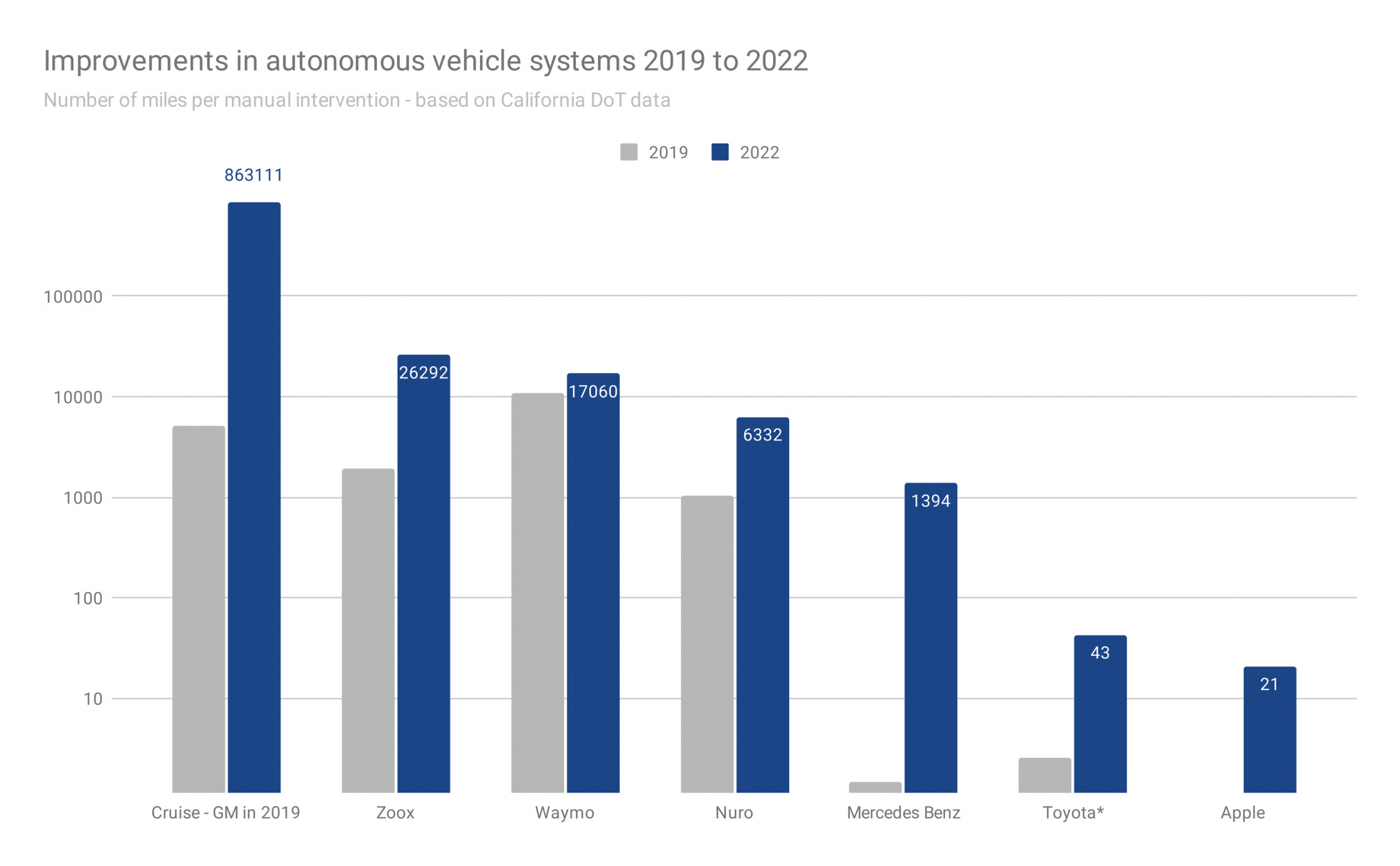
Back in 2019 we looked at the California disengagement data as part of look at the challenge self-driving cars faced over the coming years. There was a lot of variation in success with Google’s Waymo (please excuse the pun) way out in front with 11,018 miles on average per disengagement (ie the test driver grabbing the steering wheel).


As automotive ASICs play a crucial role in the decisions the car makes, we thought we’d take a look at the improvement since then.

It is impressive.


The leading AV system maker (now GM/Cruise) made travelled 863,111 miles with only 9 (nine) disenagements. Adding to the impressiveness, 8 of these were to prevent an accident caused by other drivers, and just one incidence where a “Precautionary takeover to address planning; lane keeping” was made.


And yes, like 2019, there are huge levels of variation between the disengagement rates of the system developers, there have been huge improvements all round.

Waymo is now at 17,060 miles per disengagement.

Zoox has gone from 1923 miles to 26,292 miles per

disengagement. The full data is below, with graphs showing

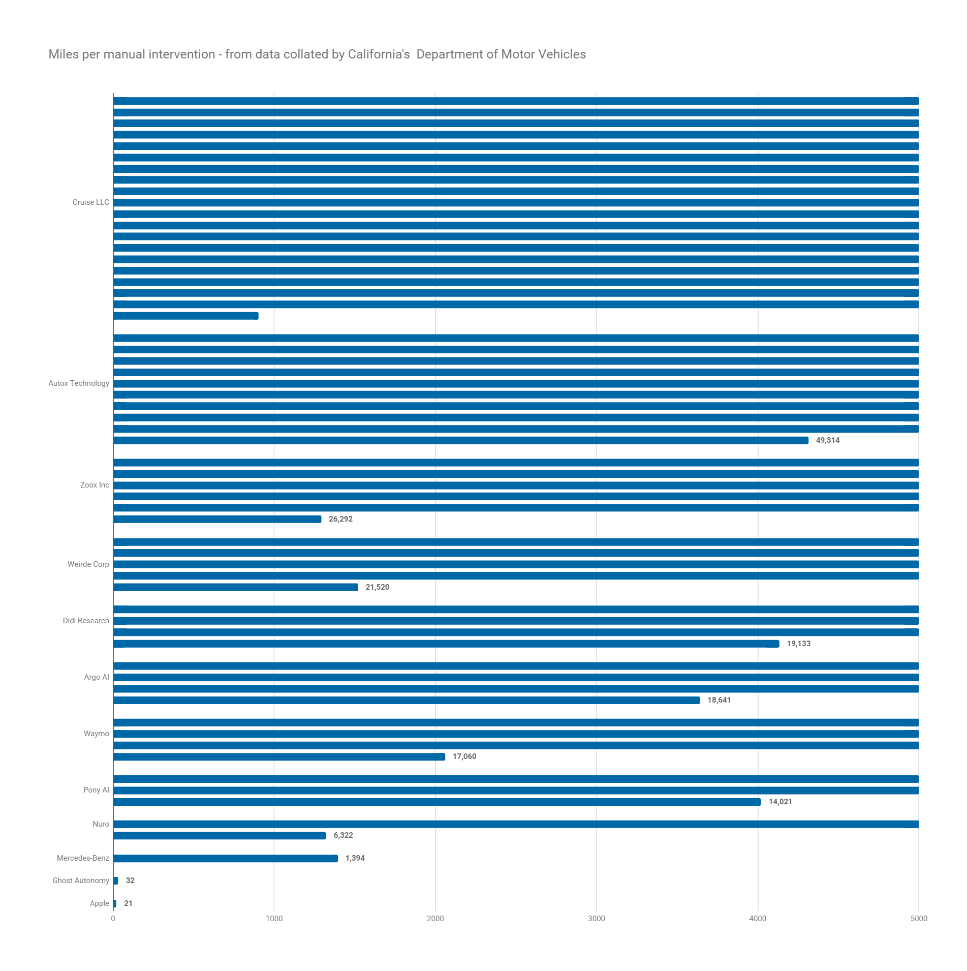
1) Miles per disengagement for all autonomous vehicle system developers and types of fault*


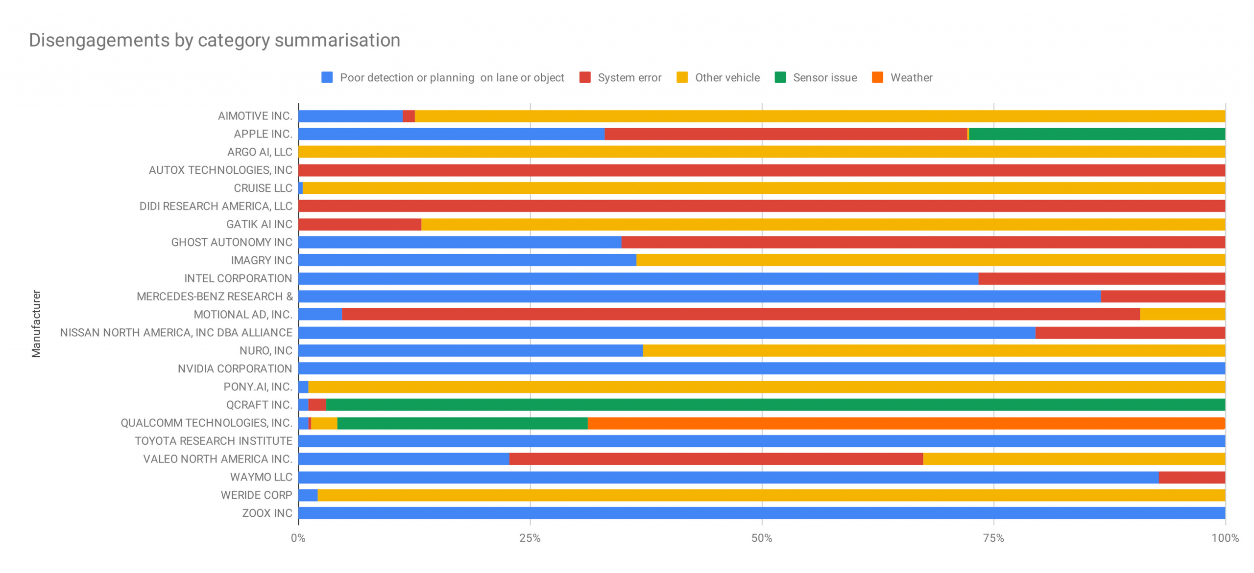
2) A breakdown showing the proportion of each class disengagement**

Advanced Strategies for RF ASICs in Space: Ensuring Functionality and Safety

In the second part of our series on designing ASICs for space applications, we build upon the foundational understanding of the environmental challenges and initial mitigation strategies outlined in part one. In this article, we shift our focus toward advanced mitigation techniques, particularly emphasizing the intricacies of RF ASICs, which play a pivotal role in communication and data transmission on board satellites. We will explore the sophisticated design strategies and software solutions that are essential in ensuring these ASICs not only withstand the harsh conditions of space but also maintain their critical functionality throughout their mission lifecycle.

Advanced Mitigation Techniques for Radiation

Advanced techniques are crucial for safeguarding the intricate circuitry of RF ASICs against the intense radiation in space. One such technique is the implementation of triple-redundancy flip-flops in the design. This approach, widely adopted in the aerospace industry, involves tripling critical circuit elements to ensure that a single radiation-induced error does not compromise the entire system. While this method significantly enhances reliability, it also increases the ASIC’s size and power requirements, a trade-off that must be carefully considered, especially in power-sensitive applications like satellite communications. These design choices are instrumental in protecting RF ASICs from single-event upsets, a common radiation-induced failure in space.


Another advanced strategy involves the use of specialized materials and shielding to further protect against radiation. Materials that can absorb or deflect high-energy particles help reduce the risk of radiation damage to the ASICs. Designers also often employ layout techniques that increase the separation between critical nodes in the circuit, reducing the likelihood of radiation-induced cross-talk or interference, which is particularly vital in the precise operations of RF ASICs. These material and layout considerations, combined with robust design strategies, form a comprehensive approach to mitigating the harsh effects of space radiation, ensuring that RF ASICs can reliably perform their functions in the challenging environment of outer space.


Software Strategies for Predicting and Fixing Errors

In the high-radiation environment of space, software strategies play a critical role in predicting and correcting errors in RF ASICs. Advanced error detection and correction algorithms are integrated into the ASICs’ firmware, allowing for real-time identification and rectification of faults caused by radiation. This is particularly important for memory components, where a single bit flip due to radiation can lead to significant data corruption. Error Correction Code (ECC) is commonly employed in these scenarios, providing an additional layer of data integrity and reliability, essential for maintaining the continuous and accurate operation of satellite communication systems.


Furthermore, software routines are designed to regularly monitor the health and status of the ASICs, implementing self-test procedures that can identify potential issues before they escalate into critical failures. This proactive approach to error management is complemented by redundancy in software operations, where critical processes are duplicated and continuously compared for discrepancies. Such strategies ensure that even in the event of a radiation-induced error, the system can maintain its operational integrity, a vital aspect for the long-term success of missions relying on satellite and RF ASICs.


Coping with Non-Ionizing Radiation

Non-ionizing radiation in space, though less discussed, poses its own set of challenges for RF ASICs, primarily through displacement damage. This type of radiation gradually alters the physical structure of semiconductor materials, leading to a progressive decline in performance. For RF ASICs, this can manifest as a gradual loss of efficiency in signal processing or increased noise levels, which can significantly impact the quality of satellite communications. To counteract these effects, designers often incorporate larger, more robust components that can tolerate gradual degradation over time, or they implement redundant systems to take over as primary components begin to show signs of wear.

Additionally, careful monitoring of voltage and current levels in RF ASICs can provide early warning signs of displacement damage. By setting thresholds for these parameters, the system can trigger alerts or switch to backup circuits when abnormal readings are detected. This approach is particularly effective in preventing sudden failures and ensuring the continuous operation of critical satellite functions. The layout of silicon tracks in these ASICs is also adjusted, with increased spacing between critical nodes to reduce the risk of damage from non-ionizing radiation, ensuring the long-term reliability and functionality of these essential components in the harsh environment of space.


The advanced mitigation techniques and software strategies we’ve covered are integral to ensuring the functionality and safety of RF ASICs in the challenging environment of space. These comprehensive approaches underscore the importance of meticulous design and proactive error management in maintaining the reliability and effectiveness of space-bound technology, essential for the success of any space mission.


Designing RF ASICs for Space: Understanding the Environmental Challenges of Satellite-Based Electronics

In the first installment of this two-part blog series on space-based ASICs, we delve into the intricate challenges of designing ASICs for the demanding environment of space. The stakes are high; launching and maintaining satellite equipment in orbit is a costly endeavor, so ensuring the effectiveness and reliability of integral components is paramount.


In this article, we’re focusing on the unique environmental challenges that ASICs used on satellites encounter beyond the Earth’s atmosphere. Unlike their terrestrial counterparts, these specialized circuits must withstand extreme conditions that go far beyond the usual demands of electronic components. From the intense radiation to the unforgiving vacuum of space, every aspect of their design demands meticulous attention to detail and precision. This is where the resilience and ingenuity of satellite ASICs truly shine, paving the way for space-based innovation and observation.


Satellite Orbiting Earth.

Satellite Orbiting Earth. 3D Scene. Elements of this image furnished by NASA.


The Unique Environment of Space for Satellite ASICs

The environment of space presents a range of challenges that are vastly different from those on Earth, posing unique hurdles for the design and functionality of RF ASICs on satellites. One of the most significant factors is the extreme temperature variations that space-bound equipment must endure. Unlike the more controlled terrestrial environments, satellite-mounted ASICs can be exposed to temperatures ranging from the intense cold of deep space to the searing heat when exposed to direct sunlight. This extreme range, which can fluctuate by as much as 150°C, demands robust design considerations to ensure the operational integrity and longevity of the ASICs in such fluctuating conditions.


Another critical aspect unique to space is the vacuum environment. This absence of atmosphere affects not only the thermal management of satellite ASICs but also impacts material selection and structural design. In space, the lack of air means that traditional cooling methods through air convection are ineffective, necessitating reliance on thermal radiation for heat dissipation. This shift requires a different approach to thermal management, with a focus on radiation and insulation techniques. Additionally, the vacuum of space can lead to outgassing from materials, potentially causing delamination or other forms of degradation. Ensuring that ASICs are designed with these factors in mind is crucial for their successful operation in the harsh and unforgiving environment of space.


Understanding Radiation and Its Impact on Satellite ASICs

A critical challenge in the design of an RF ASIC destined for space is the management and mitigation of radiation, a pervasive and potentially destructive force in the extraterrestrial environment. Space radiation primarily comprises high-energy particles, including protons and electrons from solar winds and cosmic rays from distant galaxies, which can have severe effects on electronic components. These particles, when interacting with the delicate structures of ASICs, can lead to various forms of damage, such as the buildup of charged particles in the gate oxides of transistors, altering their operational characteristics. In the realm of satellite ASICs, this can manifest as changes in threshold voltages in transistors, potentially leading to malfunction or failure of the circuit. The impact is more pronounced in smaller gate sizes, common in modern ASIC designs, where the probability of radiation-induced damage is significantly higher. Understanding these radiation effects is not only crucial for the initial design but also for the ongoing reliability and functionality of satellite ASICs operating in such a high-radiation environment. This understanding forms the basis for developing effective mitigation strategies to protect these sophisticated components from the harsh realities of space radiation.


Mitigation Techniques Part 1: Design and Material Considerations

When it comes to satellite ASICs, effective mitigation against the harsh radiation of space is achieved through a blend of innovative design and strategic material selection. For RF ASICs, which are integral in communication and signal processing in satellites, the choice of gate material and structure is pivotal. Materials that offer higher resistance to radiation help in reducing the vulnerability of these ASICs to radiation-induced damages, such as threshold voltage shifts, which are critical in maintaining signal integrity and performance. The physical design of the ASICs, including the layout and sizing of the gates, is also tailored with radiation resilience in mind. This is particularly important for RF ASICs, where precision and reliability in signal processing are paramount.


What’s more, the overall packaging of these ASICs plays a vital role in radiation protection. Utilizing radiation-hardened packaging materials and specialized insulation techniques provides an additional defense layer, crucial for shielding the sensitive electronic components from direct radiation exposure. This approach is especially relevant for RF ASICs, as it ensures the integrity and efficiency of communication systems, which are often the lifeline of satellite operations. These design and material considerations form the cornerstone of the development of robust satellite ASICs, ensuring their operational effectiveness and longevity in the challenging environment of space.


Stay tuned for our next blog, where we will delve deeper into advanced mitigation techniques and explore the crucial role of software strategies in safeguarding ASICs against the unpredictable nature of space.


*The opening image of the James Webb Space Telescope is credited to NASA/Desiree Stover.


ensilica open sign

London Stock Exchange welcomes EnSilica plc to AIM

EnSilica is a designer and supplier of mixed signal ASICs (Application Specific Integrated Circuit). ASICs are Integrated Circuits or semiconductor chips developed for a particular use or product rather than for general purpose usage.  ASICs help differentiate products through optimised hardware making products smaller, faster, lower power, improved security, add novel functionality, improving supply chain security and protecting product from being copied.


The Company has expertise in the area of designing complex mixed signal ASICs. Mixed signal ASICs combine digital and analogue functions onto a single chip. They are the most complex chips to design hence the highest value.

The Company was established in 2001 as a specialist consultancy designing ICs on a contract basis. Using over 15 years’ first-hand industry experience, the Company was able to begin transitioning to a fabless design and supply business model in 2016. EnSilica now provides an end-to-end service for the design and supply of ASICs, outsourcing certain elements such as the wafer fabrication of the manufacturing and packaging to third parties – otherwise known as a Fabless Semiconductor Model. This is a proven model for growth and profitability used by many European companies including Dialog Semiconductor, Cambridge Silicon Radio, Wolfson and Nordic Semiconductor.

EnSilica’s customers currently range from global corporations and OEMs to technology start-ups, including automotive Tier 1s, industrial enterprises, as well as large software companies and service providers developing proprietary hardware.  EnSilica is an approved supplier to some of the world’s largest automotive and industrial OEMs and Tier 1 suppliers.

Transaction Details

EnSilica, a leading designer and supplier of mixed signal ASICs (Application Specific Integrated Circuit), is pleased to announce its admission to trading on the AIM market of the London Stock Exchange. Dealings on AIM are expected to commence at 8.00 a.m. on 24 May 2022, under the ticker ENSI and ISIN GB00BN7F1618.

In connection with Admission, EnSilica has raised £6 million through a placing and subscription of 12,000,000 Ordinary Shares at a price of 50p per share and will have a market capitalisation of approximately £37.6 million at the Placing Price.

The Directors believe that the Group has reached a stage in its development where it will benefit from a quotation on AIM and that, as well as providing the Company with the net proceeds of the Fundraising, this will:

  • enhance both transparency and international profile of EnSilica with existing and potential customers;
  • allow the Company to access equity capital creating flexibility to fund growth and support potential M&A opportunities;
  • enable EnSilica to attract, recruit and retain key employees who may be further incentivised through share option schemes ; and
  • create a platform for existing shareholders to participate in the future growth of the Company

Ian Lankshear, Chief Executive Officer of EnSilica commented:

“We are delighted to be floating EnSilica on AIM and believe this represents a major endorsement of our business.  Our quoted status will provide an ideal platform from which to accelerate a number of growth initiatives which will ultimately further expand both market reach and customer footprint.

Having developed a reputation of excellence and innovation over the past 21 years, we firmly believe our mixed signal and RF design and supply capabilities are ideally placed to further capitalise on the significant demand for ASICs across our key markets.

We are excited by the numerous opportunities that being a quoted company will bring and we look forward to further developing EnSilica over the coming years.”

London Stock Exchange Logo

EnSilica to list on London Stock Exchange’s AIM market, expected to begin trading from 24th May

OXFORD, United Kingdom –May 19, 2022EnSilica, the UK-headquartered specialist designer and supplier of mixed signal ASICs has announced it is set to be listed on the London Stock Exchange’s AIM market. Trading is expected to begin from the 24th May under the ticker ENSI.

AIM is the LSE’s market for small and medium sized growth companies, with over 1,200 companies listed on it.

In connection with the Admission, EnSilica has raised £6 million (USD 7.4m) through a placing and subscription of 12,000,000 Ordinary Shares at a price of 50p per share and will open with a market capitalisation of £37.6 million (USD 46.6m).

The company designs ASICs for system developers working across the automotive, satellite and healthcare sectors. Its CEO, Ian Lankshear said “Our quoted status will provide an ideal platform from which to accelerate a number of growth initiatives, which will ultimately further expand both market reach and customer footprint.

“Having developed a reputation of excellence and innovation over the past 21 years, we firmly believe our mixed signal and RF design and supply capabilities are ideally placed to further capitalise on the significant demand for ASICs across our key markets.”