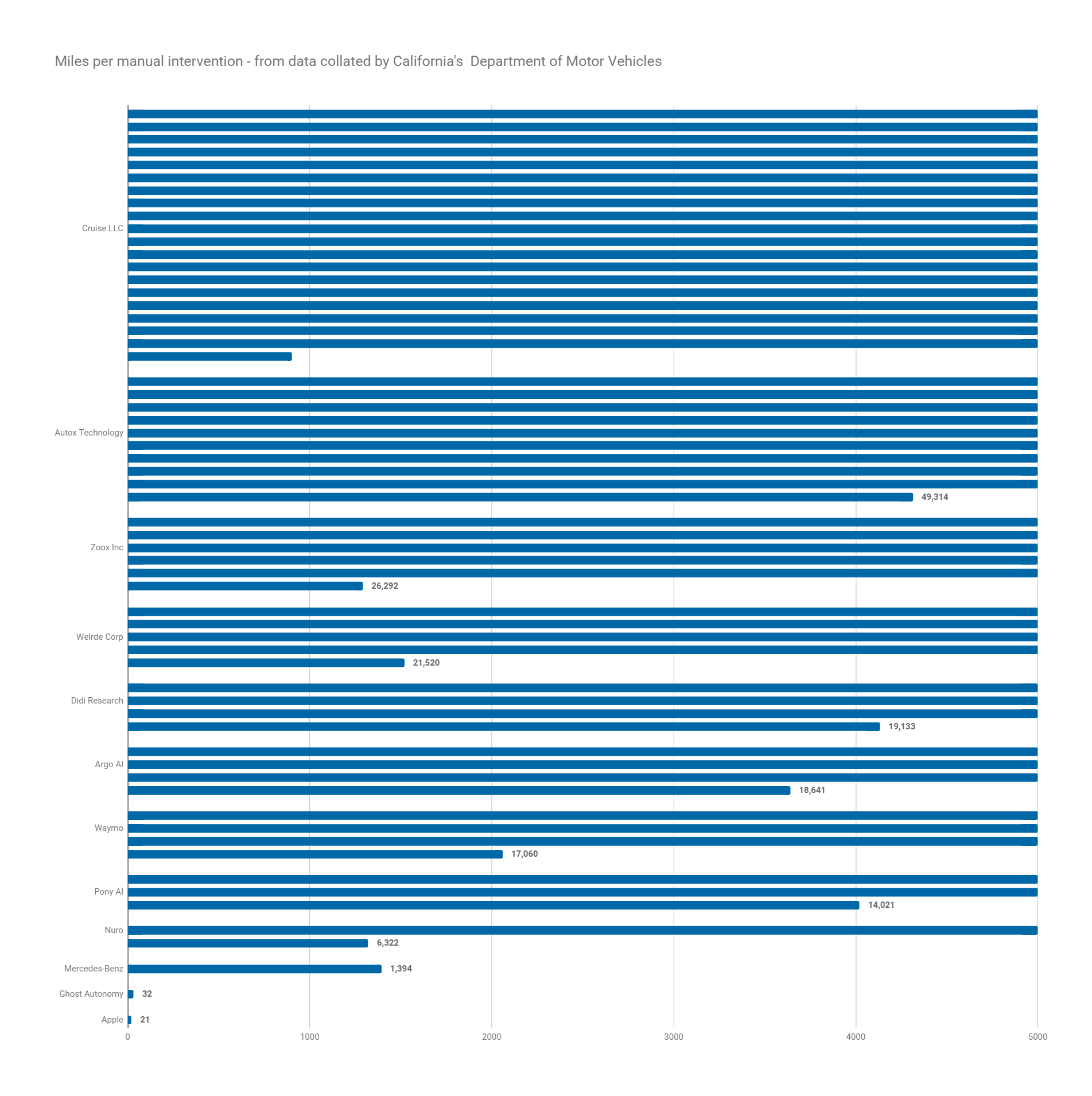
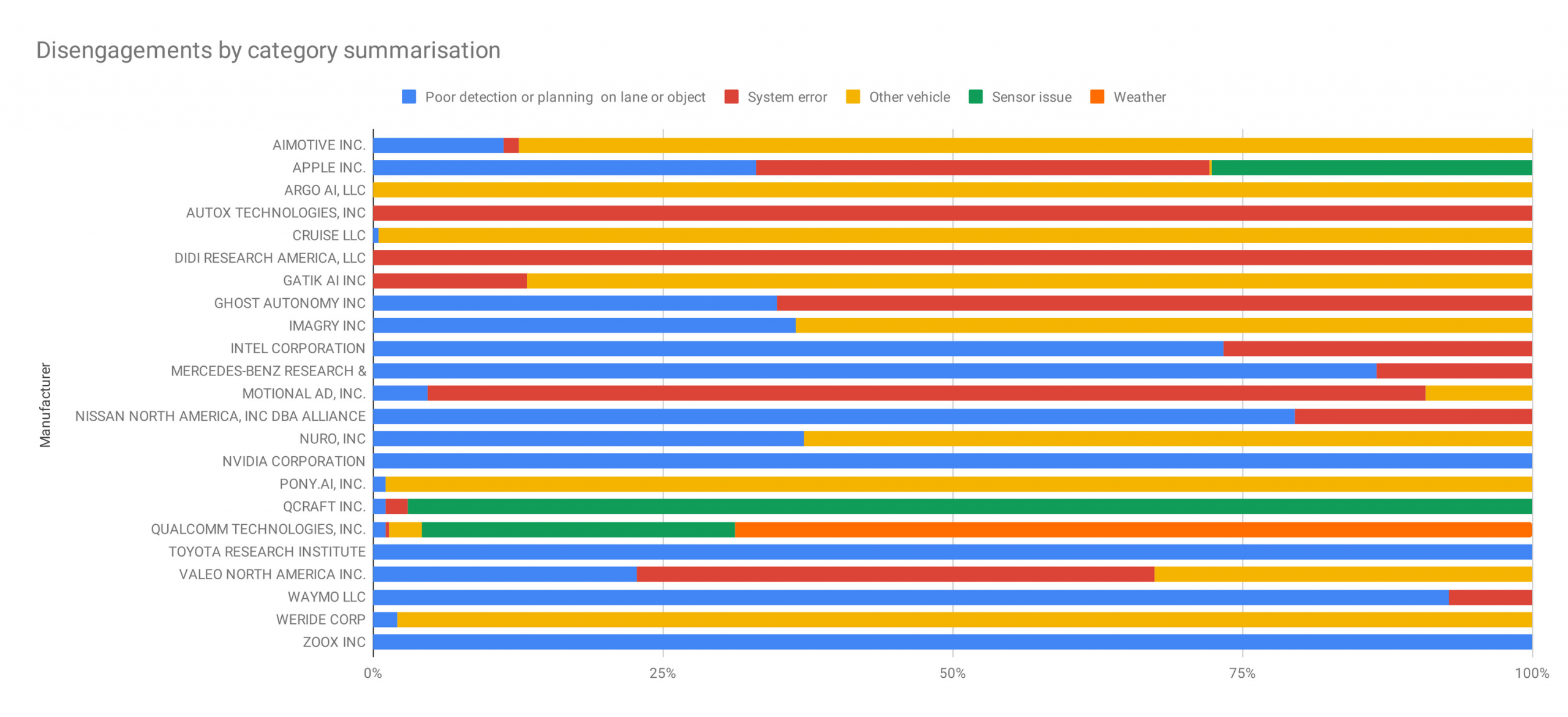
Want to see how fast autonomous vehicle ASICs have improved, look no further than the California disengagement data

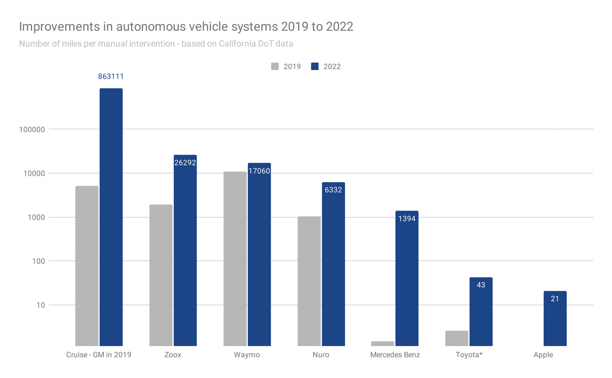
Back in 2019 we looked at the California disengagement data as part of look at the challenge self-driving cars faced over the coming years. There was a lot of variation in success with Google’s Waymo (please excuse the pun) way out in front with 11,018 miles on average per disengagement (ie the test driver grabbing the steering wheel).


As automotive ASICs play a crucial role in the decisions the car makes, we thought we’d take a look at the improvement since then.

It is impressive.


The leading AV system maker (now GM/Cruise) made travelled 863,111 miles with only 9 (nine) disenagements. Adding to the impressiveness, 8 of these were to prevent an accident caused by other drivers, and just one incidence where a “Precautionary takeover to address planning; lane keeping” was made.


And yes, like 2019, there are huge levels of variation between the disengagement rates of the system developers, there have been huge improvements all round.

Waymo is now at 17,060 miles per disengagement.

Zoox has gone from 1923 miles to 26,292 miles per

disengagement. The full data is below, with graphs showing

1) Miles per disengagement for all autonomous vehicle system developers and types of fault*


2) A breakdown showing the proportion of each class disengagement**

Advanced Strategies for RF ASICs in Space: Ensuring Functionality and Safety

In the second part of our series on designing ASICs for space applications, we build upon the foundational understanding of the environmental challenges and initial mitigation strategies outlined in part one. In this article, we shift our focus toward advanced mitigation techniques, particularly emphasizing the intricacies of RF ASICs, which play a pivotal role in communication and data transmission on board satellites. We will explore the sophisticated design strategies and software solutions that are essential in ensuring these ASICs not only withstand the harsh conditions of space but also maintain their critical functionality throughout their mission lifecycle.

Advanced Mitigation Techniques for Radiation

Advanced techniques are crucial for safeguarding the intricate circuitry of RF ASICs against the intense radiation in space. One such technique is the implementation of triple-redundancy flip-flops in the design. This approach, widely adopted in the aerospace industry, involves tripling critical circuit elements to ensure that a single radiation-induced error does not compromise the entire system. While this method significantly enhances reliability, it also increases the ASIC’s size and power requirements, a trade-off that must be carefully considered, especially in power-sensitive applications like satellite communications. These design choices are instrumental in protecting RF ASICs from single-event upsets, a common radiation-induced failure in space.


Another advanced strategy involves the use of specialized materials and shielding to further protect against radiation. Materials that can absorb or deflect high-energy particles help reduce the risk of radiation damage to the ASICs. Designers also often employ layout techniques that increase the separation between critical nodes in the circuit, reducing the likelihood of radiation-induced cross-talk or interference, which is particularly vital in the precise operations of RF ASICs. These material and layout considerations, combined with robust design strategies, form a comprehensive approach to mitigating the harsh effects of space radiation, ensuring that RF ASICs can reliably perform their functions in the challenging environment of outer space.


Software Strategies for Predicting and Fixing Errors

In the high-radiation environment of space, software strategies play a critical role in predicting and correcting errors in RF ASICs. Advanced error detection and correction algorithms are integrated into the ASICs’ firmware, allowing for real-time identification and rectification of faults caused by radiation. This is particularly important for memory components, where a single bit flip due to radiation can lead to significant data corruption. Error Correction Code (ECC) is commonly employed in these scenarios, providing an additional layer of data integrity and reliability, essential for maintaining the continuous and accurate operation of satellite communication systems.


Furthermore, software routines are designed to regularly monitor the health and status of the ASICs, implementing self-test procedures that can identify potential issues before they escalate into critical failures. This proactive approach to error management is complemented by redundancy in software operations, where critical processes are duplicated and continuously compared for discrepancies. Such strategies ensure that even in the event of a radiation-induced error, the system can maintain its operational integrity, a vital aspect for the long-term success of missions relying on satellite and RF ASICs.


Coping with Non-Ionizing Radiation

Non-ionizing radiation in space, though less discussed, poses its own set of challenges for RF ASICs, primarily through displacement damage. This type of radiation gradually alters the physical structure of semiconductor materials, leading to a progressive decline in performance. For RF ASICs, this can manifest as a gradual loss of efficiency in signal processing or increased noise levels, which can significantly impact the quality of satellite communications. To counteract these effects, designers often incorporate larger, more robust components that can tolerate gradual degradation over time, or they implement redundant systems to take over as primary components begin to show signs of wear.

Additionally, careful monitoring of voltage and current levels in RF ASICs can provide early warning signs of displacement damage. By setting thresholds for these parameters, the system can trigger alerts or switch to backup circuits when abnormal readings are detected. This approach is particularly effective in preventing sudden failures and ensuring the continuous operation of critical satellite functions. The layout of silicon tracks in these ASICs is also adjusted, with increased spacing between critical nodes to reduce the risk of damage from non-ionizing radiation, ensuring the long-term reliability and functionality of these essential components in the harsh environment of space.


The advanced mitigation techniques and software strategies we’ve covered are integral to ensuring the functionality and safety of RF ASICs in the challenging environment of space. These comprehensive approaches underscore the importance of meticulous design and proactive error management in maintaining the reliability and effectiveness of space-bound technology, essential for the success of any space mission.


Medical ASICs: Balancing Power and Performance in Wearable Technologies

When it comes to medical devices, navigating the intricate world of ASICs is something of a tightrope walk. Each step of the design phase involves striking a delicate balance between power, efficiency, and performance, where every gain comes at a cost. Medical ASICs are the beating hearts of potentially life-saving devices that must remain operational around the clock, yet are constrained by the finite capacity of their batteries. In this first part of our two-part blog series, we explore the nuanced tradeoffs that define ASIC design in medical applications, focusing on the harmonization of “always-on” functionality with the critical limitations of power resources, and how these factors interplay to shape battery size and device performance.

Balancing “always on” demands with battery capabilities

The need for “always on” functionality is now commonplace, but nowhere is it more crucial than in the development of wearable medical devices. This presents a formidable challenge when it comes to designing medical ASICs, where high performance meets the stark reality of limited battery capabilities. That’s why custom ASICs, the linchpins in these medical devices, are increasingly engineered with a keen focus on striking this critical balance. But it’s not easy. The battery’s capacity, a finite resource, automatically becomes the defining factor for the device’s energy management and overall functionality. This limitation is even more acute in devices that eschew traditional batteries for innovative energy-harvesting solutions.


However, there are ways of managing this trade-off, particularly when it comes to the strategic decision-making around the device’s duty cycle. Despite the “always on” label, an optimally designed medical device actually spends much of its time in a low-power state, conserving energy by remaining dormant until needed. This is where the ingenuity of custom ASICs shines, employing power gating as an essential tool to control leakage current in transistors – a persistent issue in medical ASICs.


The solution often lies in creating multiple clock and power domains within the ASIC, allowing power to be judiciously supplied to specific subsystems only when necessary. Typically, the most consistently active elements are a low-power timer and a memory buffer, which periodically activate the front-end circuitry for brief data conversion and storage tasks. This selective engagement, a hallmark of sophisticated ASIC design, is pivotal in marrying the necessity of “always-on” functionality with the stringent power limitations that are a hallmark of modern medical devices.


Optimizing performance with limited battery size

The pursuit of high performance in medical ASICs often leads designers into something of a struggle with battery size. High-resolution Analog-to-Digital Converters (ADCs), a staple in many medical devices for their accuracy and dynamic range, typically employ a sigma-delta architecture. This architecture, while cost-effective and precise, can be a significant drain on power resources. The challenge here is to achieve the necessary performance without imposing undue demands on the battery.


In sigma-delta ADCs, a digital filter section effectively trades sample rate for resolution, derived from a relatively simple analog input stage. This setup is ideal for managing interference in noisy environments, common in medical applications. However, the downside is the substantial energy required not just for the oversampling and filtering by the Digital Signal Processor (DSP), but also for the extensive digital post-processing on the host microcontroller. Each capture cycle, therefore, becomes a power-intensive operation, exacerbated by the high latency characteristic of sigma-delta converters, especially when high resolution is desired.


A more energy-efficient approach involves tackling interference closer to its source, using mixed-signal circuitry within the ASIC to address common noise sources. This strategy allows for a cleaner, lower-rate signal to be sent to the microcontroller, reducing overall circuit activity and, consequently, power consumption. Custom DSPs integrated into the ASIC can perform digital filtering of the oversampled signal, achieving two critical goals: reducing the dynamic range requirement for the ADC and enabling transmission of the filtered signal at a lower sample rate. This not only conserves power but also allows for the buffering of output samples within the ASIC, reducing the frequency at which the microcontroller needs to wake up for data processing. In some designs, only specific signal features or events, such as abnormal heart-rate readings, are transmitted, further minimizing power usage and maximizing the efficiency of medical ASICs.


Final thoughts

When it comes to designing medical ASICs, the tradeoffs between “always-on” functionality, performance, and battery size are not just challenges; they’re also opportunities for innovation and optimization. As we have explored, the key lies in intelligent design choices that balance these competing demands, ensuring that medical devices deliver on their promise of reliability and efficiency. Custom ASICs, with their ability to finely tune power states and manage energy consumption smartly, are the counterweights key to mastering this balancing act.


However, the exploration of power and performance tradeoffs is just the beginning. In the next article in this two-part series, we’ll delve into the equally critical aspects of functionality versus form factor and the balancing act between reducing the Bill of Materials (BoM) and managing costs. These considerations are pivotal in shaping the final design and effectiveness of medical ASICs, further demonstrating the nuanced complexity of ASIC design in the medical field. Remember, in this high-stakes arena, understanding and managing these tradeoffs is not just about technical proficiency; it’s about crafting solutions that ultimately enhance patient care and safety.


For more information, contact EnSilica’s expert team
London Stock Exchange Logo

EnSilica to list on London Stock Exchange’s AIM market, expected to begin trading from 24th May

OXFORD, United Kingdom –May 19, 2022EnSilica, the UK-headquartered specialist designer and supplier of mixed signal ASICs has announced it is set to be listed on the London Stock Exchange’s AIM market. Trading is expected to begin from the 24th May under the ticker ENSI.

AIM is the LSE’s market for small and medium sized growth companies, with over 1,200 companies listed on it.

In connection with the Admission, EnSilica has raised £6 million (USD 7.4m) through a placing and subscription of 12,000,000 Ordinary Shares at a price of 50p per share and will open with a market capitalisation of £37.6 million (USD 46.6m).

The company designs ASICs for system developers working across the automotive, satellite and healthcare sectors. Its CEO, Ian Lankshear said “Our quoted status will provide an ideal platform from which to accelerate a number of growth initiatives, which will ultimately further expand both market reach and customer footprint.

“Having developed a reputation of excellence and innovation over the past 21 years, we firmly believe our mixed signal and RF design and supply capabilities are ideally placed to further capitalise on the significant demand for ASICs across our key markets.”

techworks logo

EnSilica shortlisted for three UK TechWorks Awards

The votes are in for this year’s Electronics Weekly Elektra Awards and after another record-breaking year for entries EnSilica is proud to have its eSi-ADAS Radar Co-Processor nominated as a finalist in the “Excellence in Design” category.

date icon

EnSilica are Recruiting !

EnSilica are recruiting ! Due to our continuing growth– particularly in the area of mixed-signal ASIC development, we have a number of exciting opportunities at our UK design centres in Wokingham and Bristol.

EnSilica announce new sales partnership with Beyond Electronics, Israel

EnSilica have announced a new sales partnership with Beyond Electronics in Israel to  to help grow its customer footprint within the region.Beyond_electronics

Beyond will be offering the full range of EnSilica IPs to customers within Israel including eSi-RISC (16/32 bit embedded processor) , eSi-Crypto, eSi-Comms and eSi-Connect IPs. Beyond will also help EnSilica to expand its design service activities within the country.

“EnSilica has been highly successful in selling its IP across a number of countries over the past few years and by partnering with Beyond Electronics we are looking to replicate that same success within the Israeli market.  Beyond Electronics work with many of the most exciting and innovative companies within the country and we look forward to helping those customers achieve even more success through the adoption of EnSilica IP and services” said Ian Lankshear, Managing Director of EnSilica.

Yossi Benizri, CEO of Beyond Electronics said  “EnSilica is an ambitious company, and a leader in the Processor IP Market  and we are extremely pleased they have chosen to partner with us to create a stronger presence in Israel”

About Beyond Electronics :

Beyond Electronics is a Technical sales representative company serving the semiconductor market in Israel and Europe. Our line card consists of a focused group of industry-leading suppliers supporting the  semiconductor market.

Founded in 2012, Beyond Electronics has been rapidly expanding and already recognized as a core partner by most of the OEM’s, IDMs & fabless firms in the region.

Beyond have deployed a team of strong technical sales and application professionals who possess the requisite skills and background to forge long-term partnerships between customers and suppliers.

For further information, visit http://www.beyond-electronics.com/

About EnSilica: 

EnSilica was founded in 2001 and has a strong track record of success in delivering semiconductor IP and providing ASIC and FPGA design services to semiconductor companies and OEMs worldwide. The company is a specialist in low-power ASIC design and complex FPGA-based embedded systems, including hardware and embedded software development.

Our portfolio of IP includes eSi-RISC, a highly configurable 16/32 bit embedded processor, and families of IP covering communications, processor peripherals and encryption. In addition to providing IP and turnkey ASIC and FPGA development, EnSilica also provides point services to companies with in-house ASIC and FPGA design teams. These services include system engineering, analog and mixed signal design, advanced verification using UVM, DFT and physical implementation.

The company is headquartered in the UK and has offices in India and the USA.

For further information about EnSilica, visit https://ensilica.com