FPGA System Level Design

Modern FPGA based systems have expanded in complexity.

EnSilica are skilled in working with customer marketing and engineering teams to define new features that help differentiate your product in the market through the use of FPGAs.  EnSilica can assist or take ownership of all aspects of the system-level FPGA design. Whether the requirement is for a feasibility study, algorithm analysis, we have the expertise to solve the most difficult design problems.  We have experience with the latest high level design methodologies reducing the time to market  through the use of OpenCL, Altera DSPBuilder or Xilinx Systems  Generator for DSP. For us innovation and proven technology can go hand in hand to both differentiate and lower risk at the same time.

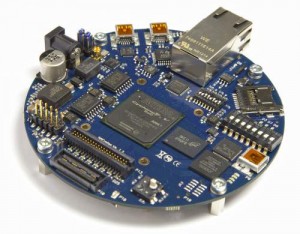
PCB2 board round

FPGA Design Services

  • Feasability Design Services

    The decisions taken at a feasibility study stage are key determining factors influencing the final product cost, FPGA selection, power consumption and interfaces. A detailed study with well reasoned choices is essential to capturing the functionality and connectivity of a design. For example the choice of connectivity has ramifications for elements as diverse as the processor subsystem and power supply.

    EnSilica has skilled System Design engineers, able to make sensible and informed decisions based on previous experience, as well as promoting novel solutions to give a competitive advantage.

  • SoC Architecture

    New digital designs invariably are a mix of software, hardware and peripherals. When it comes to software the designer has a wide choice of processor cores, some of which are technology specific, some hard, others soft, and some offering different levels of configurability to improve the requirements fit. This daunting variety is often tempered by the availability of a good toolchain and on-chip debug.

    Nevertheless the processor and its subsystem must be chosen to meet the requirements of cost and power, whilst having the compute power to perform its duties. There are many complex trade-offs of on-chip and off-chip memory that influence the efficiency of the processor. The off-chip memory could be a mix of DDR2/3 SDRAM, SRAM, SSRAM and single dual or quad ported. Some memory types can also be used in burst, pipelined or wait-stated access, depending on the memory controller, arbitration and DMA capabilities built into the SoC bus architecture. Clearly the bus architecture and processor should be jointly designed to minimise cost and maximise performance.

    EnSilica’s engineers have experience in designing complex SoC solutions for both FPGA and ASIC targets. They have a wealth of experience with bus architectures, interface peripherals such as Ethernet, USB, and PCIe, and analysing bus loading and optimizing external memory.

  • RF Systems Analysis

    The RF front end of a typical communications receiver is a complex design. The System Engineer has an overview of how the AGC, frequency, phase and analog impairment correction loop should operate, spanning the RF and digital signal processing. It is quite often the case that digital calibration can compensate for analog impairments, leading to a lower cost receiver chain, or that digital gain can be substituted for analog gain without the SNR falling below the demodulation threshold. A full analysis of receiver sensitivity and noise figure can only be carried out with knowledge of the RF and DSP performance.

    EnSilica has experienced Systems Engineers who are used to the performance trading between RF and DSP. They are familiar with the implementation of AGC, frequency, phase loops and how to compensate for RF and analog impairments.

  • DSP Alogorithms

    The use of DSP is all pervasive yet for many engineers DSP is still a black art and this forces them to consider well documented solutions. One such example may be to choose a simple FIR filter because the design tools for these are commonly available. There can be instances where different filter architectures present lower cost, latency or higher performance whilst still meeting the original requirements. This knowledge and optimization is not restricted to simple filters but extends to all areas of digital signal processing. Choosing the DSP algorithm to fit the application is still an area requiring specialist knowledge. The skill to research and apply a novel DSP solution can provide key resource minimisation on-chip, such as memory or multipliers. There are a number of tools, such as MATLAB, and SystemC that can be used to map floating point DSP into fixed point for hardware implementation.

    Within the design team at EnSilica we have DSP experts who are familiar with all the latest techniques for mapping DSP algorithms to hardware. In particular the choice of algorithm is often best made with the hardware implementation in mind, so that FPGA or ASIC resources can be best utilised.

© Copyright - EnSilica | Privacy Notice | Call Us - UK General : +44 118 321 7310 - UK Sales : +44 118 380 5757 - USA : +1 855 642 1070 - India : +91 80 2258 4450