EnSilica Agrees $18m Design and Supply ASIC Contract with European Industrial Customer

Oxford, UK

EnSilica, a leading chip maker of mixed signal ASICs (“Application Specific Integrated Circuits”), is pleased to announce that it has been awarded an $18m design and supply contract by a leading European based supplier of electromechanical products for a Cortex M series Arm-based mixed signal sensor interface ASIC to be used across a range of automotive and industrial applications. The total value of the contract is estimated to exceed $18m over seven years.


EnSilica has been selected due to its significant experience in developing mixed signal design ASICs, alongside a proven track record of bringing automotive and industrial chips to high volume production.

The part will be qualified to the stringent automotive standard AEC-Q100 grade 0 and EnSilica’s in-house functional safety flow will be used to design the ASIC to meet the requirements defined in ISO26262 Automotive Safety Integrity Level B (ASIL-B).


Ian Lankshear, CEO of EnSilica, commented: “This is another exciting design win that enhances our growing portfolio of ASICs and further improves the visibility of our recurring revenues from chip supply. This new European customer is highly respected in the industry and has a strong track record of shipping its products in high volume. This contract is a testament to the company’s ability to deliver high-quality, reliable solutions that meet the evolving needs of the market and further demonstrates our team’s commitment to excellence and innovation which continues to drive our success and position EnSilica as a premier European ASIC supplier.”

EnSilica Opens Second Brazilian Design Centre Following Multimillion Pound Design and Manufacturing Contract Win


Oxford, UK

EnSilica, a leading maker of mixed-signal ASICs, has opened a second design centre in Brazil after a series of design wins, the most recent being a multimillion-pound design and manufacturing contract from an optical computing systems customer. The new design centre is in Campinas, São Paulo State, and complements the company’s Porto Alegre facility in Rio Grande do Sul, in southeastern Brazil.


Through strengthened relationships with key wafer foundry and semiconductor supply chain partners. EnSilica increasingly provides not only design services but also wafers, packages, and tested devices. This model, which has been successfully developed by several leading Asian chip design companies, is now being leveraged by EnSilica to meet the growing demand for a resilient European-based supply chain.


Campinas was chosen for its strong semiconductor ecosystem, which has enabled rapid growth of EnSilica’s existing engineering team in the region.


EnSilica CEO, Ian Lankshear, commented: “We are pleased to secure this sizable contract with a pioneering optical computing systems company. This agreement not only underscores our capabilities in delivering comprehensive design and manufacturing services but also highlights the growing demand for European-based supply chains. Our strengthened relationships with key wafer foundry and semiconductor supply chain partners enable us to provide high-quality wafers, packages, and completed tested devices. We are also delighted to be opening our second design centre in Brazil, which further underscores our strategic ambitions to expand our global footprint in order to meet the increasing demand for our services.”

European Space Agency and EnSilica partner to enable fully integrated ASICs for resilient GNSS

In partnership with the European Space Agency (ESA), EnSilica, a leading maker of mixed-signal ASICs, will design and develop a key silicon component to enable next-generation resilient multi-band Global Navigation Satellite System (“GNSS”) capabilities. These are vital to ensuring the world’s critical infrastructure and services remain robust and secure in the face of evolving global threats.


EnSilica will design and develop a key silicon component to enable next-generation resilient multi-band Global Navigation Satellite System (“GNSS”) capabilities, which are vital to ensuring the world’s critical infrastructure and services remain robust and secure in the face of evolving global threats.


The ESA, NAVISP Element 2 programme helps to increase the competitiveness of participating European states in the global market for satellite navigation and enables these countries to be well positioned to capitalise on emerging market opportunities across Positioning, Navigation and Timing (“PNT”) technologies and services.


EnSilica has a growing satellite communications market footprint and is working with support from ESA and UKSA, with the latter organisation awarding the Company £10.38 million in February 2025 for a development project under its Connectivity in Low Earth Orbit programme. Part of the company’s expertise is in architecting and implementing systems-on-chip with high-performance RF, including mmWave, and complex baseband processing.


Paul Morris, VP RF and Communications Business Unit at EnSilica, said, “As we and our infrastructure become ever more dependent on PNT services in everyday life, it is important to have highly integrated, resilient, and precise technology sourced in Europe and the UK. This collaboration will allow us to accelerate such technology, starting with a next-generation radio design enabling our partners to focus on integrating their custom algorithms.”


Ian Lankshear, Chief Executive Officer of EnSilica, added, “I am extremely proud of our team to have been secured this agreement under the ESA NAVISP Element 2. This project will enable us to further enhance global navigation satellite systems technology and continue to develop commercial solutions that are critical for resilient and reliable satellite navigation. We are grateful for the ongoing support from ESA and the UKSA, and we continue to focus on PNT and the broader satellite communications market as a key growth driver of our business.”


UK Space Agency Awards EnSilica £10.38m for Satellite Broadband Terminal Chips

EnSilica (AIM: ENSI), a leading chip maker of mixed signal ASICs (Application Specific Integrated Circuits), announces that it has been awarded funding from the UK Space Agency under its Connectivity in Low-Earth Orbit (“C-LEO”) programme. Following a competitive selection process, EnSilica has been awarded £10.38 million over the next three-years for a development project pioneered by EnSilica.


EnSilica put forward in its application a compelling business case, supported by letters of interest from potential lead customers, to develop a family of semiconductor chips to support future generations of best-in-class, highly integrated, mass market satellite broadband user terminals. The terminals will be capable of connecting with various satellite constellations and will leverage advanced semiconductor technology. In addition, the project will provide a resilient and secure source of chips which is independent and not tied to specific satellite service operators.


The market potential for satellite user terminals is growing rapidly, as demonstrated by Starlink, and is projected to reach c. US$16.5 billion by 20311. Each terminal requires hundreds of specialist chips to create an electronically steerable antenna.


The UK Space Agency’s C-LEO programme was launched last year and is designed to ensure that the UK space sector remains competitive in the rapidly evolving global market for low-earth orbit constellations. With a total funding pool of up to £160 million available over the next four years, the C-LEO programme supports the development of smarter satellites, enhanced hardware, AI-driven data delivery, and improved inter-satellite connections.


This new project builds on EnSilica’s successful history of collaboration with the UK Space Agency and the European Space Agency, alongside other key satellite communications partnerships and the company’s own investment in the technology.


Paul Morris, EnSilica VP RF and Comms Business Unit, commented: “This is a great opportunity to accelerate our chipset development enabling us to extend our portfolio of chips for the satellite broadband market with a focus on providing a complete solution for user terminals while reducing cost and power.  We are now engaged with the key European players and I’m sure this further backing from the UK Space Agency will help us garner global interest in the unique products we are developing.”


Ian Lankshear, EnSilica’s CEO, commented: “We are honoured and proud to have won this highly significant award from the UK Space Agency under the C-LEO programme, as we believe satellite communications is an incredibly important sector for EnSilica and one that is fast expanding globally. This funding will enable us to advance our technology and bring innovative solutions to the satellite broadband market, with the project expected to be hugely beneficial to society, offering resilient internet connectivity in times of crisis, as well as providing high speed internet connectivity in remote communities not well served by terrestrial networks. We welcome the ongoing support from the UK Space Agency, which provides the framework for EnSilica to develop the technology required to address a market worth many hundreds of millions.”


EnSilica joins TSMC Design Center Alliance

We are proud to announce that EnSilica has joined the TSMC Design Center Alliance (DCA). This significant achievement underscores our deep expertise in mixed signal and RF design, now combined with TSMC’s advanced technology to deliver unparalleled solutions to our mutual customers.

EnSilica is committed to providing high-performance ASIC solutions across the automotive, industrial, healthcare, and communications sectors using TSMC technologies. Whether you need high-quality full turnkey ASICs or a comprehensive range of services—from PDK access, design support, MPW shuttles, production tape-out, and wafer supply, to packaging, test development, qualification, and supply chain management—we are here to be your trusted IC Partner.

Read the full press release here.


EnSilica: Leading the Way in FinFET Technology

In the dynamic landscape of wireless communication, semiconductor innovations play a pivotal role. Among these, FinFET technology stands out as a game-changer. Let’s explore how FinFETs are shaping the future of 5G and satellite communication.

MIMO Systems: A Brief Overview

Deployment of 5G terrestrial and satellite communications relies heavily on the integration of Multiple-Input, Multiple-Output (MIMO) systems to meet the link budget requirements and mitigate interference.

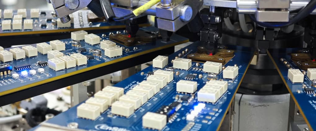
Fin field-effect transistors (FinFETs), represent a departure from traditional planar transistors. Their three-dimensional fin-like structure allows for better control over current flow, reducing the leakage and improving power efficiency. This technology has been the key enabler for the design of highly integrated digital radio ASICs, based on RF ADCs and DACs, supporting multiple standards.

Key Changes with FinFETs

  1. Improved RF and Analog performance:
  • FinFETs exhibit superior Gm and Rout characteristic, which is paramount to implement the highly linear analog signal processing required in MIMO systems.
  • Excellent RF performance with fT values of 600GHz.
  • MIMO signals remain pristine even in challenging environments.
  1. Power Efficiency Boost:
  • The subthreshold slope of FinFET devices is practically ideal. This drastically reduces leakage current—the silent power drain—that has plagued semiconductor devices for years.
  • For 5G devices and satellite communication terminals, where power constraints are stringent, FinFET-based designs shine.


Design Challenges

Despite the improvements in performance, FinFET technology introduces complexity in the design that impact the work of engineers and their approach to RF ASICs.

Now more than ever analog designers, who delve into the intricacies of FinFET, need accurate modelling to ensure that their designs align with the theoretical predictions. Rigorous simulations validate performance metrics, allowing for confident deployment.

At the same time designers face a delicate balancing act. Performance, power consumption, and chip area—these factors intertwine. Effective trade-offs lead to optimized designs that meet real-world requirements.

Impact on Satellite Communication

  • Custom ASICs empower cost-effective, low-power satellite broadband user terminals.
  • These terminals, based on MIMO communication systems, enable seamless connectivity, even in remote areas. Collaborations with space agencies underscore the commitment to advancing satellite communication technology.
  • Hybrid satellite/5G networks are on the horizon, promising ubiquitous connectivity.

The journey through the FinFET landscape is one of innovation, precision, and impact. As we embrace the future of wireless communication, semiconductor advancements remain a beacon—a testament to human ingenuity.


For more in-depth insights, please refer to the full article in the Microwave Journal by EnSilica’s FinFET expert Gabriele Devita

EnSilica adds Post Quantum Cryptography support to eSi-Crypto IP library

First license for EnSIlica’s PQC cores licensed to major semiconductor vendor for 5nm networking chip

OXFORD, United Kingdom – January 15th 2024 – EnSilica (AIM: ENSI), a leading chip maker of mixed-signal ASICs, has added a range of Post-Quantum Cryptography (PQC) accelerators to its eSi-Crypto range of hardware accelerator IP.

These cryptographic algorithms are developed to withstand cyber-attacks from quantum computers, and their launch makes EnSilica one of very few companies to offer advanced cryptographic accelerators to the market as licensable hardware IP cores.

By implementing these in hardware cryptographic operations, such as encryption and decryption, can be performed faster, with lower-power and more securely than software-based implementations.

The first license for EnSilica’s new QPC cores has now been granted to a major semiconductor company for target at a high performance 5nm networking chip.

Why PQC is essential:
Today’s secure communications and financial transactions rely on public-key encryption techniques. These use maths problems a conventional computer cannot readily solve. However, advances in both quantum computing and artificial intelligence-based systems, which are backed by large datasets that need to be kept secured, means there is a real threat that cyber-attacks will break current standards.

As such, the U.S. Department of Commerce’s National Institute of Standards and Technology (NIST) published its first draft standard for encryption algorithms capable of resisting quantum attacks in H2 last year. for the first of these cryptographic algorithms was published by the last year, with feedback completed in November.

In its 2023 announcement, the NIST mathematician Dustin Moody, who led the seven-year project to develop the algorithms said their creation meant “We’re getting close to the light at the end of the tunnel, where people will have standards they can use in practice”

EnSilica’s PQC accelerator IP:
EnSilica has added two new PQC accellerators to its eSi-Crypto range of IP:

• eSi-Dilithium is a hardware IP designed for accelerating the NIST FIPS 204 Module Lattice Digital Signature Algorithm called CRYSTALS Dilithium
• eSi-Kyber is a hardware IP designed for accelerating the NIST FIPS 203 Key Encapsulation Mechanism (KEM) called CRYSTALS Kyber.

Dilithium and Kyber algorithms are both part of the Cryptographic Suite for Algebraic Lattices (CRYSTALS) and are based on the computational difficulty of the Module Learning With Errors (MLWE) problem.

Additionally, the eSi-SHA3 has also been added to eSi-Crypto, this is a hardware IP designed for accelerating the NIST FIP 202 cryptographic hashing algorithms including SHA3 and SHAKE

These add to and complement EnSilica’s existing range of non-quantum resistant cryptography accelerators, which include ECC, EDCDA, RSA, AES, DES/3DES, SNOW3G, ChaCha20 and Poly1305 as well as a NIST compliant True Random number generator (TRNG). The cores are suitable for ASIC and FPGA usage and can be pre-configured to meet a range of throughputs and compatible with a range of AMBA buses including APB, AHB and AXI.

The timely adoption of PQC is driven by the concern that sensitive encrypted data harvested today, might one day be compromised once powerful quantum computers emerge. This is a critical security risk for governments safeguarding secrets and businesses handling sensitive and confidential information.


Ian Lankshear, Chief Executive Officer of EnSilica, commented:
“EnSilica’s commitment to technological innovation is reflected in our comprehensive range of cryptographic accelerators IP to address the next generation of cybersecurity threats.

The licensing agreement with this major semiconductor giant validates the intrinsic value of our intellectual property. EnSilica not only licenses its IP to other semiconductor companies but also leverages it in the development of custom ASICs.”

Paul Morris, VP RF and Comms Business Unit, commented:
“EnSilica’s PQC cores will be a critical IP when we are building the next generation communication ASICs for our customers, enabling us to build in robust defences against quantum threats. With quantum-resistant algorithms, PQC not only ensures data integrity and confidentiality but also bolsters non-repudiation, preventing denial of digital signatures and affirming the authenticity of communications in the quantum era.”.

Bernard Wu, VP Sensing and Control Business Unit, commented:
“The cybersecurity landscape is evolving necessitating for the redesign of many ASICs due to the recently enacted EU Network and Information Security (NIS2) legislation. The NIS2 directive, now encompassing industrial and manufacturing sector as well as transportation. Our new QPC IP along with our existing range of non-quantum resistant cryptography accelerators provide us with the technology to secure our customers ASIC so they are fit being supplied well into the next decade.”

EnSilica’s Vasiliki Xiradaki named among UK’s best young engineers in a trio of prestigious industry awards

TechWorks/UK Electronic Skills Foundation

Electronic Weekly’s BrightSparks Awards

The IET Future Talents Scholarship.


EnSilica’s Vasiliki Xiradaki was named among the UK’s top 3 student electronic engineers at the annual TechWorks industry awards  ceremony on the 7th December. The award category, run and presided over by the UK Electronic Skills Foundation follows hot on the heels of Xiradaki being declared among the UK’s 30 best engineers under 30 in Electronics Weekly’s BrightSparks Awards, which was presented just one week earlier on the 30th November.


Completing a hat trick of awards, this month has also seen Xiradaki be awarded Future Talents Scholarship by the IET.


EnSilica CEO Ian Lankshear said: “We’re delighted for Vasiliki and so proud of her, the awards are so very, very deserved.


“Helping young, talented engineers to develop and flourish is an exceptionally important part of our culture and these two awards coupled with Omotade Iluromi winning last year’s TechWork’s Young Engineer of the Year Award are testament to the support given here.”


Xiradaki has been working with EnSilica as an UKESF scholar since for 13 months and is in her 3rd year of an electronic engineering degree at the University of Birmingham. At EnSIlica Xiradaki has played an active role in the company’s satellite communications IC projects, working on both verification and on module design for projects including a Satellite Communications on the Move chip to give commercial, military and disaster recovery vehicles access to high-speed communications anywhere on the planet.


Outside of EnSilica, Xiradaki is an advocate for women in engineering and for engineers from diverse backgrounds. For this, she has been actively participating in many outreach activities across different age groups, visiting more than 10 schools to help bring under-represented groups of people into STEM subjects and electronic engineering degrees. This has helped her be selected by the UKESF to participate in the Academy Achiever’s #BeMeDigitalInclusion charity STEM event which is targeted at black girls from vulnerable backgrounds.