NEWS ARTICLE
Article first published in Electronic Design on 28th July 2021; by EnSilica’s Patrick McNamee (Director of Silicon Operations) & David Tester (Director of Engineering)
The automotive electronics market has traditionally been dominated by a small handful of big tier-1 suppliers that have a long-established supply chain. The rise of electric and driverless vehicles means that this is changing rapidly, and non-tier-1 suppliers are no-longer left with the slim pickings of aftermarket and infotainment systems.
Here Patrick McNamee and David Tester of the ASIC design house EnSilica look at some of the key takeaway lessons smaller suppliers can implement from one recent project.
The move to electric, and more recently ADAS, vehicles has turned what was a very established, static industry on its head. As has been written about (ourselves included), this provides opportunities for smaller electronic system vendors outside of the “tier-1” club to gain inroads into the automotive supply chain. This transition, coupled with the speed of innovation required by the automotive manufacturers, means that many of the traditional tier-1 suppliers will often lack the necessary skills to create solutions for these new technologies: creating the gap for new and innovative companies to enter.
Earlier this year, EnSilica announced a new custom automotive ASIC had completed the final PPAP and Part Submission Warrant declaration (PSW) entered mass production – going through the design and certification in less than 24 months.
In this case our customer was the tier-1 supplier, working with them to fill the gap in their skillset and support their OEM customer. For sensitivity and confidentiality reasons we will not name either.
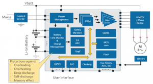
The part in question was a complex mixed-signal ASIC that uses a BCD process with high-voltage transistors, and combines extensive monitoring and fault detection circuits with duplicate redundancy on key functions and was created to be used in EVs albeit the technology is equally suited to hybrids, and hydrogen fuel-cell powered vehicles.
In addition to the well understood AEC-Q qualification, which is undertaken over three production lots and extensive reliability testing, this design was designated safety critical and had to follow a study of safe launch planning and the use of part average testing in manufacturing. The Safety aspect also led us into the design methodologies and audits as prescribed in ISO 26262, all of which we had to learn from scratch.
Here we summarize some of the key elements of the project that will help you take advantage of the opportunity.
The challenge faced
Before we begin, a bit of background.
The primary issue for this particular ASIC was time, the tier-1 supplier’s timescale was very aggressive by automotive standards, and this was exacerbated by the need for high analog complexity (including high voltages and extreme precision), which meant few ASIC design agencies had the required skills.
A secondary challenge was cost. The OEM exclusively makes high-end luxury vehicles, which means the volumes of ASICs produced are smaller than if they were used in a more mass-market brand such as Ford or BMW, and with that comes reduced economies of scale, meaning costs need to be well managed.
How we selected the supply chain
EnSilica is a relatively small fabless ASIC vendor, and we therefore had to first come up with a credible supply chain that would demonstrate to the customer that we could manage them and get the appropriate support to a high-volume automotive component.
Most of the large wafer foundries offer an automotive option on their mainstream processes. This (typically) means a smaller list of equipment is used, with tightened in line process controls to reduce the likelihood of defects and, perhaps more importantly for automotive, to reduce batch-to-batch variation. Assembly vendors also operate similar automotive variants for the packaging schemes.
This left the decision of where to do the test development and the qualification. Test and qualification of this kind of device requires the collection of a lot of data over a large number of tests. It is done over three wafer production lots and tens of thousands of devices. All of it needed to be undertaken in parallel with our own, and the customer’s, design verification.
Unlike process and packages where we are essentially buying a well-proven product, the entirety of the qualification and characterization cycle is all unique to this project. After some evaluation we chose a supplier that could support all these activities in one location and could demonstrate a track record in doing this kind of project with small fabless companies.
What we had to learn from a device perspective
As an ASIC vendor we routinely develop digital and mixed-signal ASICs for a range of customers across safety and non-safety critical applications, including automotive. However, this vehicle manufacturer was new to EnSilica and required us to very quickly understand both the system-level functionality and the company’s concerns. Understanding the fine detail of complex systems takes time, we had no option but to perform this system-level learning, with this task undertaken by our modelling group in parallel with our silicon group running the ASIC component-level development.
Expertise can embed yourself higher up the supply chain too
EnSilica has end-to-end expertise covering digital IC design, analog IC design and systems design. We used this to engage with both the tier-1 and the vehicle manufacturer in as many areas as possible – not just on the ASIC definition and development, but on the ECUs (which would be made by the tier-1 supplier) definition and development too.
What we had to learn about designing for safety (26262 references)
The end application was safety critical, and the ASIC was required to support the ASIL-D safety level. In addition to the core functionality, considerable additional safety related functionality needed to be defined and implemented for the ASIC.
Much of this fault-detection functionality could only be defined and tested at the ECU system-level. Additionally, as the core component within the ECU in this safety critical application, the development process needed to be fully documented with regular FMEAs (failure mode and effects analyses) during the development and the fault metrics regularly tracked with FMEDAs (failure modes, effects and diagnostic analyses).
The journey through to first silicon
For the OEM, many aspects of the automotive ECU could only be validated after silicon was available. Therefore, from the project’s start there was a race to get to first silicon. Development time for the mixed-signal ASIC was eight months with a three-month silicon manufacturing cycle, meaning the ASIC was soldered down in the ECU after just eleven months from project start.
Feature creep must be avoided
One of the many challenges with this project was that the detailed definition of the ASIC – the specification – needed to be written in parallel with the ASIC development work. In essence, the moment the ink dried on a section of the ASIC specification then the design work for that part of the ASIC commenced. Taking this approach means that feature creep happens easily and avoiding this is only possible by using system-level modelling undertaken by a small, highly focused team.
Pre-qual should be undertaken
It was always intended, given the tight timescale, to create a specification and initial design that could undergo a partial redesign in order to get the device fully centered. But this also means that, unless you can be sure that these changes would be minor and not affect form fit or function, you are not allowed to start your automotive qualifications, which require final production tooling.
To solve this, without wasting time between first and final silicon, we undertook a cut down version of an AEC-Q qualification that looked at the riskier sections: the burn-in, early-life failure rate (ELFR), package integrity discharge (ESD) and latch up (LU). To do this required significant cost to design and procure the necessary tooling. We would say that this is, however, money well spent, and in this case it uncovered a small number of potential issues with the product’s design and manufacture that needed improvement before going to final silicon.
Second silicon and qualification
First samples of the final version of the silicon were delivered to Ensilica at the beginning of April 2020, just as the Covid-19 pandemic had forced most of the world into lockdown. This kicked off a large number of parallel activities including:
- Design evaluation inside EnSilica
- Design evaluation by our customer
- Debugging ATE program to get a release candidate to test all the samples required for AEC-Q100 qualification.
- Planning and execution the full schedule of tests over the three production lots as required.
- Full PVT characterization and correlation to end application
- PPAP and PSW delivery
Summary
Lessons learned
We learned much on this journey at many levels, the three most important takeaway lessons, to me, were:
- Ensuring a frequent and detailed technical information exchange, and a review that encompassed the entire ECU design, not just the ASIC.
- Having a tight and detailed internal design and specification review process particularly as we were aware that feature creep was inevitable given the timescales.
- The pre-qual that we performed on first silicon, although seeming costly at the time, was vital in getting to final silicon faster
I could not really complete this article without discussing the impact of Covid on the latter stages of qualification and test development. I can say with certainty that not being able to travel to the test and qualification partner for more than a year has definitely impacted the efficiency of the project and led to some basic errors and misunderstandings that have in turn caused delay or extra work.
Yet despite this, we were still able to complete the final PPAP and Part Submission Warrant declaration (PSW) entered mass production in less than 24 months from starting the project, demonstrating that there are opportunities for smaller electronic system vendors to gain inroads into the automotive supply chain as the move to electric and ADAS vehicles continues, turning what was a very-established industry on its head.

