
Managing tradeoffs in ASIC design for low-power, small-form-factor wearable medical devices
Here EnSilica’s Konstantinos Glaros examines some key tradeoffs OEMs will likely face
when taking an ASIC approach and how to balance these tradeoffs more effectively.
Wearable technology for healthcare and wellness applications represents a tremendous opportunity. The potential designs range from smart plasters through wrist monitors to therapeutic systems. But a common set of constraints unites many of these devices, the most important of which are accuracy, energy usage, size and cost. Though each of these has an important bearing on the hardware design, the tradeoffs that designers need to face will often focus primarily on the device’s energy profile. How power consumption changes with activity frequently dominates architectural decisions and the degree to which design can satisfy the other constraints.
Tradeoff 1: Always on vs battery size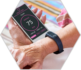
The capacity of an attached battery will restrict the energy that can be supplied to the device. Battery-less designs that employ energy harvesting will be even more constrained. The energy limitation will control several aspects of the design. From a system-design standpoint, the decision with the greatest impact at all levels is that of the duty cycle.
Though many healthcare devices present themselves as “always on”, for much of the time an efficient design will ensure most of the circuitry will run on a low duty cycle: asleep and powered down for as long as possible before being called into action. In modern process nodes, power gating is essential, to prevent the constantly flowing leakage current in powered transistors. Implementing multiple clock and power domains, for example, ensures power is supplied only to the subsystems that need it at the right time.
Many times, the only part of the system that is active at all times is a highly power-efficient timer and memory buffer that periodically wakes the front-end circuitry to perform a data conversion and move the data into the buffer. Circuitry or firmware may monitor the incoming data to see if certain thresholds have been exceeded or if the buffer is full. If so, the logic can trigger a state transition that wakes up a supervisory microcontroller to analyze the data. Decisions made at that level may lead to more parts of the system being woken up to take further action. That action may take the form of relaying data to another IoT device or smartphone host over Bluetooth.
Though the sleep and wake cycles can be managed at the software or firmware level, this is not necessarily optimal for power efficiency. This is one reason using a front-end ASIC can deliver a significant advantage when full-system power consumption is considered. A front-end ASIC can often provide the ability to fine-tune control of power states that may not be available in the predefined states of an off-the-shelf front-end data converter.
Tradeoff 2: Performance vs battery size
Many off-the-shelf high-resolution ADCs employ a sigma-delta architecture.  In this architecture, a digital filter section trades sample rate for resolution from a relatively simple analog input stage, a design approach that provides high accuracy and dynamic range at relatively low cost in modern semiconductor processes. The high dynamic range can help manage interference in healthcare devices, where there is often significant noise mixed in with the signal of interest.
Digital signal processing of the captures by a relatively powerful processor can filter out much of the noise and interferers from what may be a relatively small signal of interest. Unfortunately, this combination of strategies leads to a power-hungry system. Significant energy is not just required for the oversampling and filtering performed by the DSP, but also in the extensive digital post-processing needed on the host microcontroller, which may need to be active for each capture. This issue can be exacerbated by the high latency of sigma-delta converters when decimation filters are scaled up to achieve high resolution. The time required to obtain each block of samples from the start of the capture sequence can lead to an increase in the duty-cycle ratio of the host microcontroller/system.
A more energy-efficient solution is to focus on handling interference closer to the source and use mixed-signal circuitry to deal with common noise sources so that a cleaner, lower-rate signal can be relayed to the host microcontroller. This type of design often employs custom DSP on the ASIC to carry out the digital filtering of the oversampled signal for two purposes. By removing the effects of large interferers at the source, it is possible to reduce the dynamic range requirement for the ADC. Second, the filtered signal can be transmitted to the microprocessor using a lower sample rate, which reduces circuit activity and, consequently, power. Further savings can be made by buffering some output samples in memory on the ASIC, waking the microcontroller at infrequent intervals to read them out and process them. At the limit, only specific signal features or events, such as an abnormal heart-rate value, may be transmitted, to be logged, or wake up the system for further action. As the output sample rate is now low, further power savings can also be gained by storing the output samples in memory on the ASIC and only waking up the microcontroller very infrequently to read them out.
With less need for high dynamic range, the resulting ASIC can, in turn, employ a far less energy-intensive conversion architecture. It may still be a sigma-delta converter, but one that employs a simpler, lower-latency decimation filter stage. Such a design has a shorter startup overhead which lends itself to faster power-up and power-down cycles or multiplexing across input channels. Another option is a successive-approximation (SAR) design, as this is an architecture that delivers high energy efficiency overall. For slowly changing inputs, a charge-integrating circuit may offer the best combination of energy usage, resolution, and capture rate.
Tradeoff 3: Functionality vs form factor?
An important characteristic of front-end ASICs is that they can be very space efficient. It is common for the silicon to measure less than 3 x 3mm, making the devices highly suitable for the small package sizes of healthcare wearables. However, the use of chip-scale packages that take full advantage of the ASIC’s compact nature will cause a limited number of I/O connections from the device. This works in opposition to the trend of building more sensor inputs into the system. Multiple inputs provide the ability to probe more skin sites in order to obtain a better signal. Smart healthcare wearables are increasingly combining data from different sensor modalities to improve overall results and, at the same time, deal more effectively with noise from individual inputs.
A conventional method to balance the tradeoff between chip size and an increase in I/O connections is to move to packages that offer a higher pitch density than the standard pitch of 0.4mm. The trade-off is that this will probably increase overall system cost because of changes that will be needed in the PCB and assembly technology to handle the finer-pitch circuit traces. Another option is to increase the level of multiplexing on I/O channels, particularly for connections to an external microcontroller.
Multiplexing over serial ports provides an efficient way of trading pin count against data throughput. There is flexibility in terms of which protocol to use. If it can support the device’s required data rate, using two-wire I2C rather than four-wire SPI frees up two potentially precious I/O pins.
A further source of saving in terms of pin count is through circuit design techniques that avoid the need to use external passives, such as capacitors and inductors, to handle analog-processing functions. Mixed-signal processes offered by foundries allow passive elements to be formed in the metal interconnect stack and can provide an effective trade off of die size against pin count.
It’s also worth mentioning that advanced packaging techniques will also free up PCB real estate and IO pins by embedding both the analog front end and sensors in a single package.
Tradeoff 4: Reduced BoM vs cost?
In an ideal world, most of the functions of a system would be absorbed into a single ASIC. But there are several cases where this would not be economically viable.
What functions are integrated into an ASIC and the process node the ASIC will need to implement them will be affected by a huge number of requirements. They include voltage levels, IP availability, support for nonvolatile memory, the number of logic gates required, and cost. Analog interfaces and other support circuitry will often show better economics on mature process nodes with transistors and other integrated components not scaling as logic or memory transistors do.
You may not be able to have everything you want, but a good ASIC designer will be able to balance tradeoffs and look at the complete system to find you the best option.
A good example of the tradeoffs at work is a glucose monitoring patch. This type of device needs an analog front-end, BLE support for wireless communications, a processor core and flash memory. Assuming a 55nm target process, the total ASIC development cost could reach several million US dollars. This would not just be for the design and creation of the masks used for production at the fab, but licensing the BLE and processor IP.
A more cost-effective way of approaching the same design would be to use an analog front-end ASIC that is designed to work with a variety of off-the-shelf BLE-enabled processors. The flexibility to support different external processors would allow manufacturing changes if supply-chain conditions demand it.
Doing so would demand duplication of some functions in the ASIC, possibly requiring additional general-purpose I/O and I2C or SPI interfaces, together with power-management interfaces. This may add to the ASIC’s size and therefore cost. But bigger savings could be achieved. The ASIC would be able to use a mature process with lower mask costs, such as 130nm. And the ASIC would require less IP to be licensed, which will reduce the development cost. But the architecture would still deliver supply-chain protection.
Conclusion
Taking an ASIC approach gives protection from supply chain issues and allows you to optimize your design. But there are always tradeoffs, and these should be understood before taking this route.

