The chip, which will be initially available with evaluation boards, has been created to meet the needs of a diverse array of home-use and single-use medical sensors – from oximeters to smart plasters – as well as wearable healthcare sensors and fitness trackers.
According to EnSilica, the IC is among the first of its kind to integrate an NFC energy harvesting circuit, making it suitable for both battery-powered and battery-less systems.
A modular IC design has been implemented in the ENS62020, which allows for the customisation of the ENS62020 and enables a product-optimised ASIC while greatly reducing the time to market.
EnSilica CEO, Ian Lankshear said, “EnSilica is focused on developing ASICs in close collaboration with our customers. The ENS62020 was born out of requirements coming from a number of customers that were seeking to develop differentiated products in this fast-growing wearable healthcare and medical device market.”
According to figures provided by Deloitte, the wearable medical sensors market is forecast to grow at 19% CAGR to 2024, with 280 million smart watches/fitness trackers and 160 million wearable medical sensors shipping in 2024.
The ENS62020 healthcare sensor interface IC supports the accurate and reliable measurement of an array of vital signs including: ECG, temperature and differential capacitance, as well as optical signals, which are used to track heart rate, oxygen saturation (SpO2), glucose levels and for near-infrared spectroscopy.
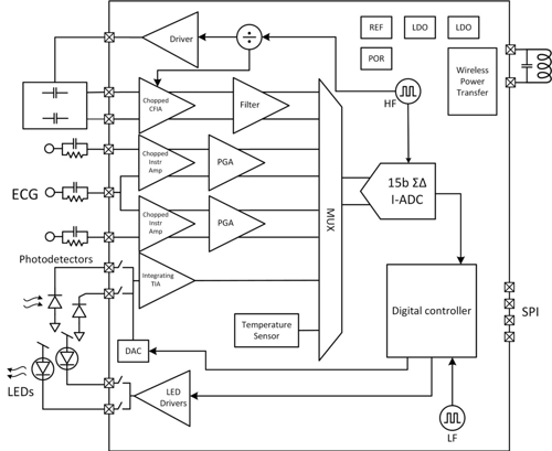
According to EnSilica, due to the size and power-optimised design, the device is suited to disposable medical devices and patches as well as sports and fitness devices. The highly sensitive capacitive sensor interface also makes the device well suited for novel MEMS sensors.
The IC is designed to work alongside an edge processor, or a communication device, and incorporates two photodiode drivers/photodetector readouts; two differential ECG sensor channels suitable for 3-lead ECG with <1.6µVrms noise levels; a highly sensitive capacitive sensor channel; a temperature sensor with <0.15oC resolution (between 35-45oC); a low-power ADC. The device consumes from just ~10µA per sensor.
The device will come in a plastic QFN 32-pin package, with samples available from June, or as part of an evaluation kit with board and demonstration software from July.

